Electrode structure, and method for manufacturing thin-film structure

A manufacturing method and structure technology, which is applied in semiconductor/solid-state device manufacturing, electric solid-state device manufacturing, microstructure device manufacturing, etc., can solve problems such as strength problems, and achieve the goals of reducing shear stress, improving strength, and suppressing cracks Effect

Inactive Publication Date: 2004-01-07
MITSUBISHI ELECTRIC CORP
View PDF0 Cites 3 Cited by
  • Summary
  • Abstract
  • Description
  • Claims
  • Application Information

AI Technical Summary

Problems solved by technology

The occurrence of such cracks is not only a problem of its own strength, but also has a high possibility that the etchant used for the etching of the above-mentioned etching film 121 reaches the first insulating film 113.

Method used


Image

  • Electrode structure, and method for manufacturing thin-film structure
  • Electrode structure, and method for manufacturing thin-film structure
  • Electrode structure, and method for manufacturing thin-film structure

Examples


Embodiment Construction

[0053] A. Implementation form 1

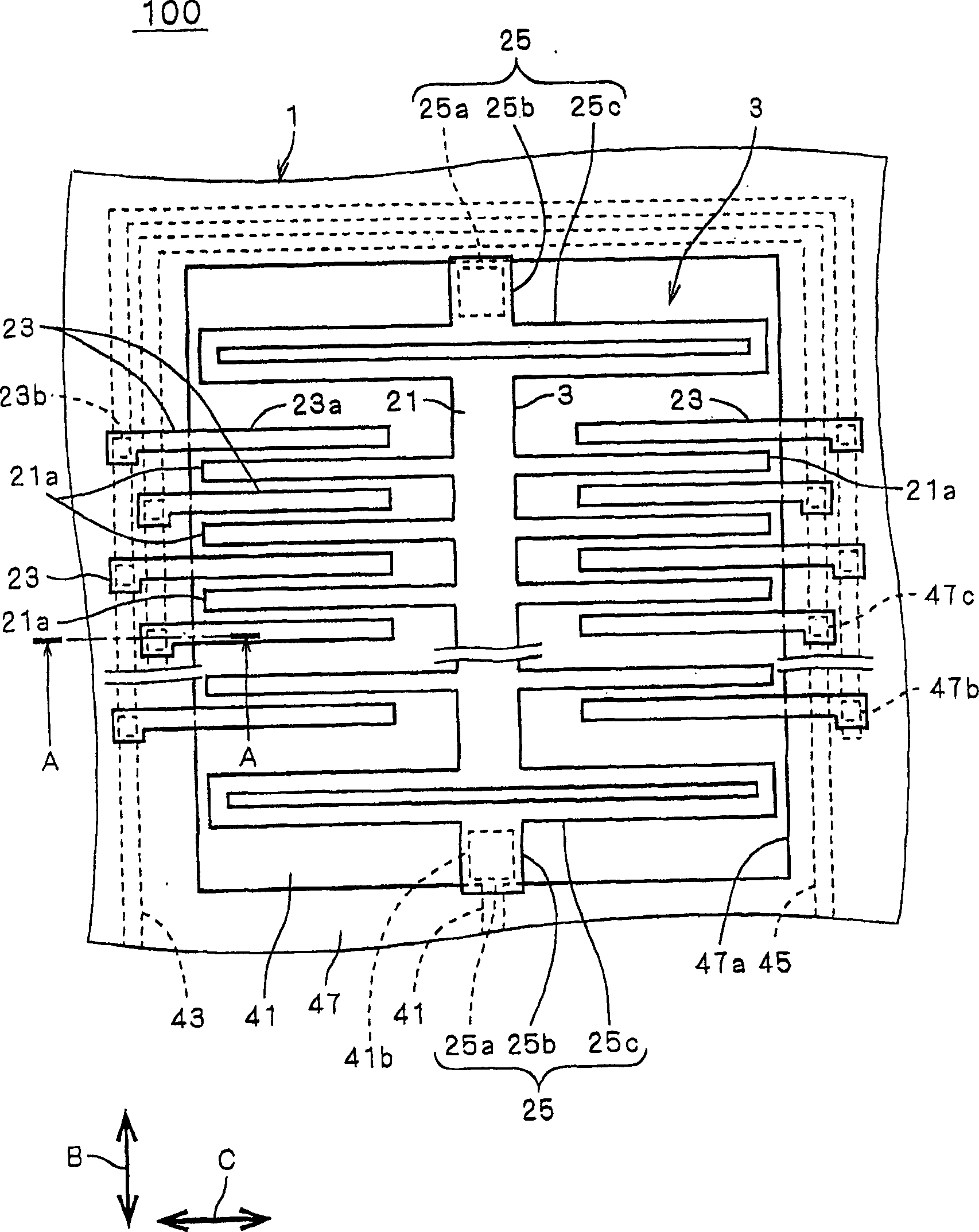
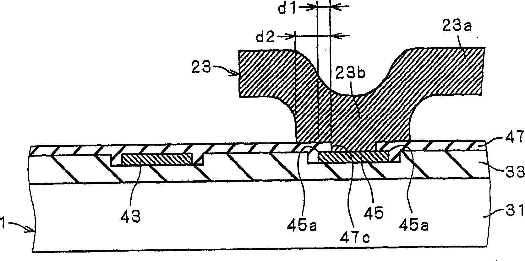
[0054] figure 1 It is a plan view showing the main part structure of the semiconductor acceleration sensor 100 to which the method of manufacturing the thin film structure of the present invention can be applied. figure 2 is along figure 1 The A-A line profile. The semiconductor acceleration sensor 100 includes a substrate 1 as a sensor substrate, and is formed on the substrate 1 ( figure 1 The center is the front side of the paper), and the sensor part 3 has the function of detecting acceleration.

[0055] The sensor unit 3 includes a movable mass body 21, several fixed structures 23, and several beams 25, and is formed as a thin film structure. The thin film structure is formed of a conductive material, for example polysilicon doped with impurities, for example doped polysilicon doped with phosphorus.

[0056] The mass body 21 has a plurality of movable electrode portions 21 a extending along a direction C perpendicular to the direc...


PUM


Abstract

An electrode structure where a sacrifice film is removed without removing another insulating film and a method for manufacturing a thin-film structure. There are formed anchor holes for opening the surface of a wiring line which is covered with a sacrifice film and a nitride film. The anchor hole is formed of a hole portion of the nitride film and an opening of the sacrifice film. The diameter ofthe hole portion is smaller than the width of the wiring line by a first predetermined distance from the edge of the surface of the wiring. The diameter distance from the hole portion. Because of thepresence of the first and second predetermined distances, the distance by which the etchant for removing the sacrifice film penetrate into an oxide film.

Description

technical field [0001] The present invention relates to an electrode structure formed by semiconductor processing technology and a method for manufacturing a thin film structure. Background technique [0002] Figure 17 It is a sectional view showing a conventional electrode structure, and shows a thin film structure 101 included in the electrode structure. The thin film structure 101 includes a support portion 103 and a floating portion 105 supported by the support body 103, and is formed on a substrate 107 using a conductive material. The floating portion 105 is arranged at a predetermined interval from the substrate 107 , and protrudes outward from the upper portion of the support portion 103 . [0003] The substrate 107 includes a substrate main body 111 , a first insulating film 113 , wiring 115 , and a second insulating film 117 . The first insulating film 113 is formed on the substrate body 111 . The wiring 115 is provided on the surface of the first insulating fil...

Claims


Application Information

Patent Timeline
Patent Type & Authority Applications(China)
IPC IPC(8): B81B3/00H01L21/768H01L29/84
CPCH01L2924/0002B81B2203/0307B81C1/00095B81C2201/0109H01L2924/00H01L28/00
Inventor 堀川牧夫石桥清志奥村美香
Owner MITSUBISHI ELECTRIC CORP
Why Eureka
Try Eureka