Charge pump circuit and working method using its non-volatile storage

A charge pump and circuit technology, applied in the field of non-volatile memory, can solve the problems of not being able to get negative high voltage output, not being able to get high voltage output, etc.

Inactive Publication Date: 2002-08-21
MITSUBISHI ELECTRIC CORP
View PDF2 Cites 17 Cited by
  • Summary
  • Abstract
  • Description
  • Claims
  • Application Information

AI Technical Summary

Problems solved by technology

[0015] exist Figure 20 When a positive voltage occurs, as described above, the NMOS transistor 108 is turned on due to being charged to the Vdd-Vth potential, while the PMOS transistor 109 is turned off (Vdd potential) and does not discharge to the ground 102. However, due to the positive voltage The output POUT becomes a potential higher than Vdd, so it discharges from the PMOS transistor 109 to the ground line 102, so the potential does not rise, and the desired positive high voltage output cannot be obtained.
[0016] In addition, in Figure 21 When a negative voltage of the negative voltage occurs, the PMOS transistor 109 is turned on because it is charged to the GND+Vth potential, and the NMOS transistor 108 is turned off (GDN potential). However, since the negative voltage output NOUT becomes a potential lower than GND, from The NMOS transistor 108 is charged to a potential Vdd potential higher than that of the power supply 101, and therefore, the potential does not drop, so that a negative high voltage output cannot be obtained.
[0017] In this way, although the existing charge pump circuit for generating positive and negative voltages can generate two power supplies of positive voltage and negative voltage, the desired high voltage output cannot be obtained.
[0018] In addition, when using a charge pump circuit to operate a nonvolatile memory such as a flash memory, it is necessary to apply opposite high voltages to the floating gate and the well to inject and pull electrons out. However, when positive and negative voltages occur when using Different from the case of using separate charge pump circuits for positive voltage generation and negative voltage generation, the operation method of the nonvolatile memory of the charge pump circuit of these two voltages cannot combine the positive voltage and the negative voltage Applied to wordline and well

Method used


Image

  • Charge pump circuit and working method using its non-volatile storage
  • Charge pump circuit and working method using its non-volatile storage
  • Charge pump circuit and working method using its non-volatile storage

Examples


Embodiment 1

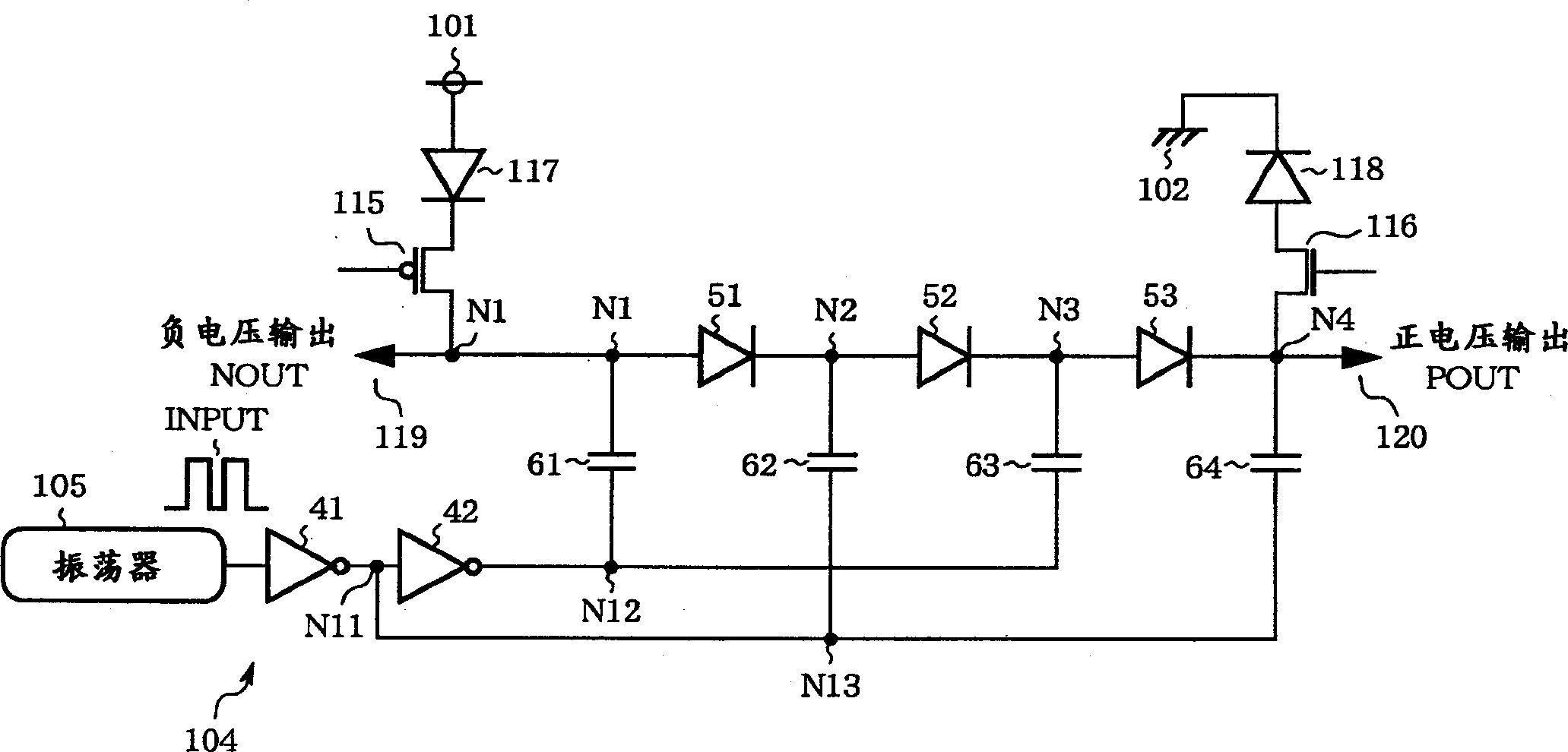
[0055] figure 1 It is a circuit diagram showing the structure of the charge pump circuit in Embodiment 1 of the present invention. In the figure, 41 and 42 are inverters, constituting the actuator 104, 51-53, 117, and 118 are diodes, 61-64 are capacitors, and 101 is a An external power supply supplying Vdd potential (first power supply potential), 102 is a ground wire supplying GND potential (second power supply potential), 105 is an oscillator, 115 is a PMOS transistor (P channel MOS transistor), and 116 is an NMOS transistor ( N-channel MOS transistor), N1-N4, N11-N13 are nodes. Diodes 51 to 53 are connected in series to form a voltage generating circuit (voltage generating unit). Nodes N1 and N4 serve as first and fourth internal nodes, respectively, connecting negative voltage output NOUT and positive voltage output POUT of the voltage generating circuit.

[0056] Here, the external power supply 101 is a power supply for the user to use the semiconductor integrated circu...

Embodiment 2

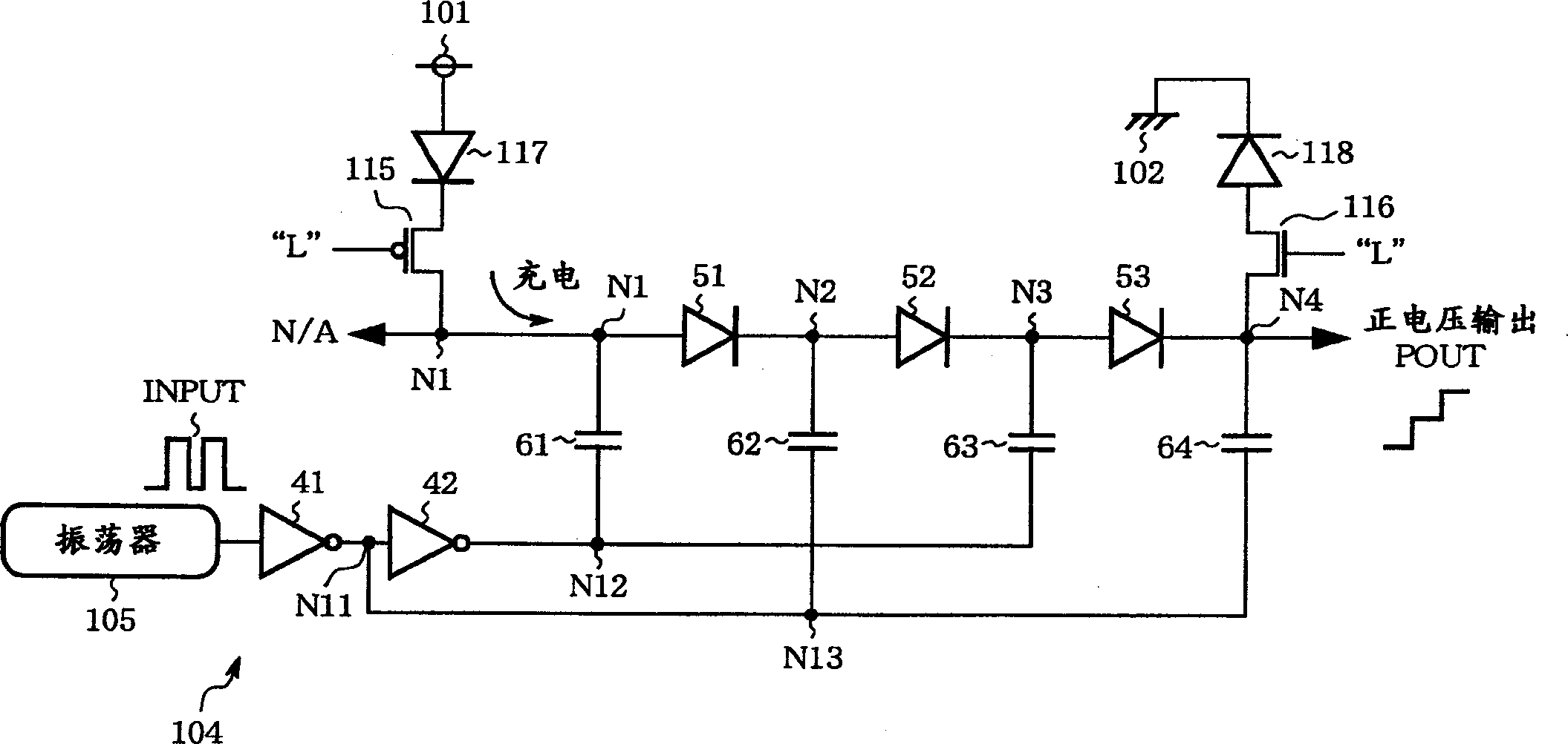
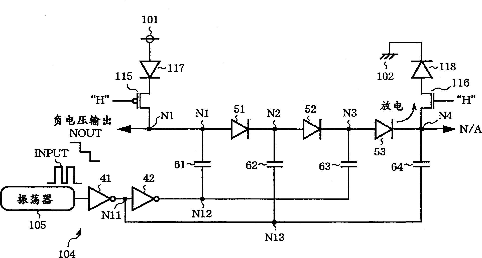
[0067] Figure 4 is a circuit diagram for illustrating problems to be considered in Embodiment 2 of the present invention, using Figure 1 ~ Figure 3 The charge pump circuit of the above-mentioned embodiment 1 is shown. in addition, Figure 5 and Image 6 These are a schematic sectional view of the first backflow prevention circuit on the external power supply 101 side and a schematic sectional view of the second backflow prevention circuit on the ground 102 side, respectively.

[0068] In the figure, 21 is an N well, 31 is a P well, 23 and 33 are gates, 22a and 22b are P+ diffusion layers, 32a and 32b are N+ diffusion layers, and other structures are the same as those in Embodiment 1 above, so the repeated illustrate. For convenience of description, DVth represents the thresholds of the diodes 117 and 118, and Vth represents the thresholds of the PN junctions between the P+ diffusion layer and the N well and between the N+ diffusion layer and the P well.

[0069]In the s...

Embodiment 3

[0077] Figure 8 is a schematic diagram for explaining problems to be considered in Embodiment 3 of the present invention, Figure 9 It is a circuit diagram showing the configuration of the charge pump circuit of the third embodiment. In the figure, Q0 is the charge amount (several pF) supplied each time, Q1 is the charge amount of the load capacitor (several pF), ΔQ is the remaining charge amount, and SW1, SW2, and SW3 are switches (the first to third switching units ), N21 is a node, 125 is a minimum unit, and other structures are the same as in the above-mentioned embodiment 1, so the repeated description thereof is omitted.

[0078] Usually, a capacitor and a diode of a charge pump circuit are the smallest unit 125, and a high voltage is generated by connecting a plurality of them in series. The larger the number of connections, the higher the voltage can be generated, and the larger the supply current can be. However, the required voltages may be different between the ...


PUM


Abstract

Traditional charge pump circuit for generating positive and negative voltages, without high voltage outputs. There is a provided a charge pump circuit comprising: a first reverse current prevention circuit connected between an external power supply and a first internal node; a first output node, connected to the first internal node, for outputting a first output potential; a second reverse current prevention circuit connected between a second power supply node receiving ground potential and a second internal node; power supply node for receiving a first power supply potential; a first reverse current prevention means connected between the first power supply node and a first internal node; a first output node, connected to the first internal node, for outputting a first output potential; and power supply generation means, connected between the first internal node and second internal node, for enhancing the potential of the second internal node as compared to that of the first internal node, wherein the power supply generation means is formed on or within a semiconductor substrate, and includes a diode element provided so as to flow a current from the first internal node to the second internal node, and a capacitor having one electrode connected to the first and second nodes, and the other electrode provided with a clock signal. thereby enabling higher outputs on both positive and negative voltages.

Description

technical field [0001] In particular, the gate semiconductor integrated circuit of the present invention is a charge pump circuit that generates a positive or negative voltage from an externally supplied power supply potential, and an operating method of a nonvolatile memory using the charge pump circuit. Background technique [0002] The power supplied to semiconductor integrated circuits from the outside is usually a single power supply or a dual power supply. However, electronic devices such as flash memories that require multiple power supplies need to generate the desired voltage internally. The circuit that performs this function is usually called a charge pump. circuit. This charge pump circuit consists of multiple capacitors, drivers, and oscillators. In recent years, with the advancement of semiconductor integrated circuits, the power supply voltage has had to be lowered in order to achieve low power consumption. Therefore, low-voltage charge amplifiers are essenti...

Claims


Application Information

Patent Timeline
IPC IPC(8): G11C16/06G11C5/14G11C16/30H01L21/822H01L27/04
CPCG11C16/30G11C5/145G11C5/14
Inventor 石井元治尾本加代子
Owner MITSUBISHI ELECTRIC CORP
Why Eureka
Try Eureka