Method for producing alignment mark

A technology of alignment marks and manufacturing methods, applied in semiconductor/solid-state device manufacturing, electrical components, circuits, etc., can solve the problems of difficult allocation of alignment marks, neglect, and increased wafer area.

Inactive Publication Date: 2006-10-11
TAIWAN SEMICON MFG CO LTD
View PDF0 Cites 3 Cited by
  • Summary
  • Abstract
  • Description
  • Claims
  • Application Information

AI Technical Summary

Problems solved by technology

However, putting the alignment marks in the wafer will increase the area of ​​the wafer, and the alignment marks are ignored when designing the wafer layout, making it difficult to add the alignment marks after the wafer is completed
On the other hand, if the alignment mark is placed on the cutting line, the position of the alignment mark will be limited by the test line (Testline), the cursor (Vernier), the critical dimension bar (CriticalDimension Bar; CD Bar), covered Patterns, and alignment marks used in photolithography, causing difficulties in dispensing alignment marks

Method used


Image

  • Method for producing alignment mark
  • Method for producing alignment mark
  • Method for producing alignment mark

Examples


Embodiment Construction

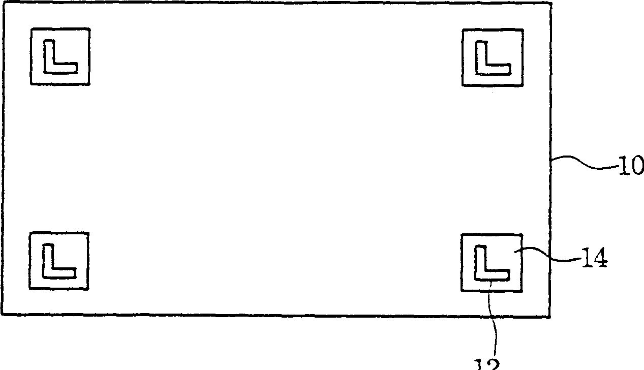
[0026] From the above-mentioned known methods of manufacturing alignment marks for laser repair calibration, it can be seen that the alignment marks are made in the wafer and the area of ​​the wafer will be increased. Lines, optical rulers, critical dimension bars, overlay patterns, and alignment marks of the photolithography process overlap, so the placement of the alignment marks will be limited, causing problems in allocation.

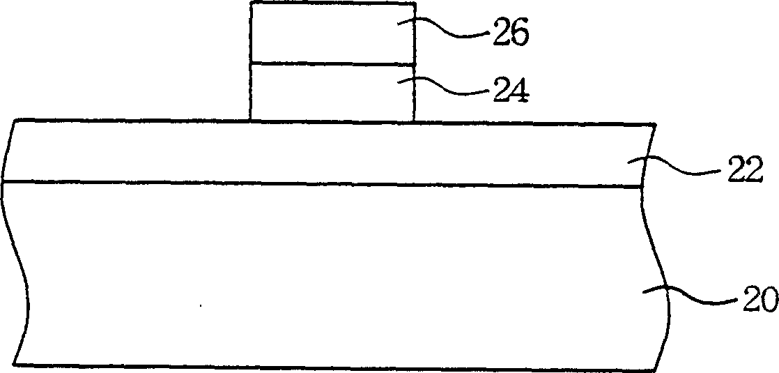
[0027] In order to reduce the wafer area and avoid the trouble caused when assigning the position of the alignment mark, the alignment mark can be made above the upper metal layer, and a dielectric layer is added between the alignment mark and the upper metal layer to prevent The occurrence of electrical short circuit. Please refer to this structure figure 2 , which has been formed with a plurality of semiconductor components on the substrate 20, covered with a first metal layer 22, wherein the first metal layer 22 can be, for example, the upper m...


PUM


Abstract

The invention discloses a method for manufacturing an alignment mark (Alignment Mark), which is to first form an inter-metal dielectric (Inter-Metal Dielectric; IMD) layer on a top metal layer (Top Metal Layer) such as an aluminum-copper alloy, and then After forming a layer of low-reflective material such as titanium nitride (TitaniumNitride; TiN), and then forming a metal layer on the low-reflective material layer, and using this metal layer to manufacture alignment marks, so the alignment marks are consistent with the underlying The light-dark contrast between the layers of low-reflective material is obvious, which facilitates the alignment of subsequent laser repairs. In addition, the low reflectivity material layer can also be used as an etching stop layer (Etching Stop Layer) of the metal layer.

Description

technical field [0001] The present invention relates to a method for manufacturing an alignment mark, in particular to a method for manufacturing an alignment mark on a top metal layer (Top Metal Layer). Background technique [0002] In the manufacturing process of semiconductor components, as the components become smaller and smaller, the photoresist pattern is also reduced. Therefore, in the photolithography (Photolithography) process, in order to transfer the photoresist pattern to the semiconductor wafer accurately, It is usually necessary to provide several alignment marks on the wafer for aligning the photoresist so that the photoresist pattern is accurately copied to the desired position on the wafer. [0003] On the other hand, in the final product testing stage, when performing laser repair (Laser Repair), in order to make the laser accurately cut off the unnecessary polysilicon fuse (Polysilicon Fuse) in the component, it is also necessary to use alignment marks to...

Claims


Application Information

Patent Timeline
Patent Type & Authority Patents(China)
IPC IPC(8): H01L21/02
Inventor 黄俊岩李建毅傅如彬彭荣义
Owner TAIWAN SEMICON MFG CO LTD
Why Eureka
Try Eureka