Liquid crystal display device
a liquid crystal display and display device technology, applied in optics, non-linear optics, instruments, etc., can solve problems such as unnoticeable defects, and achieve the effect of reducing the generation of contact failure and short circuit, and facilitating laser repair
- Summary
- Abstract
- Description
- Claims
- Application Information
AI Technical Summary
Benefits of technology
Problems solved by technology
Method used
Image

Examples
embodiment 1
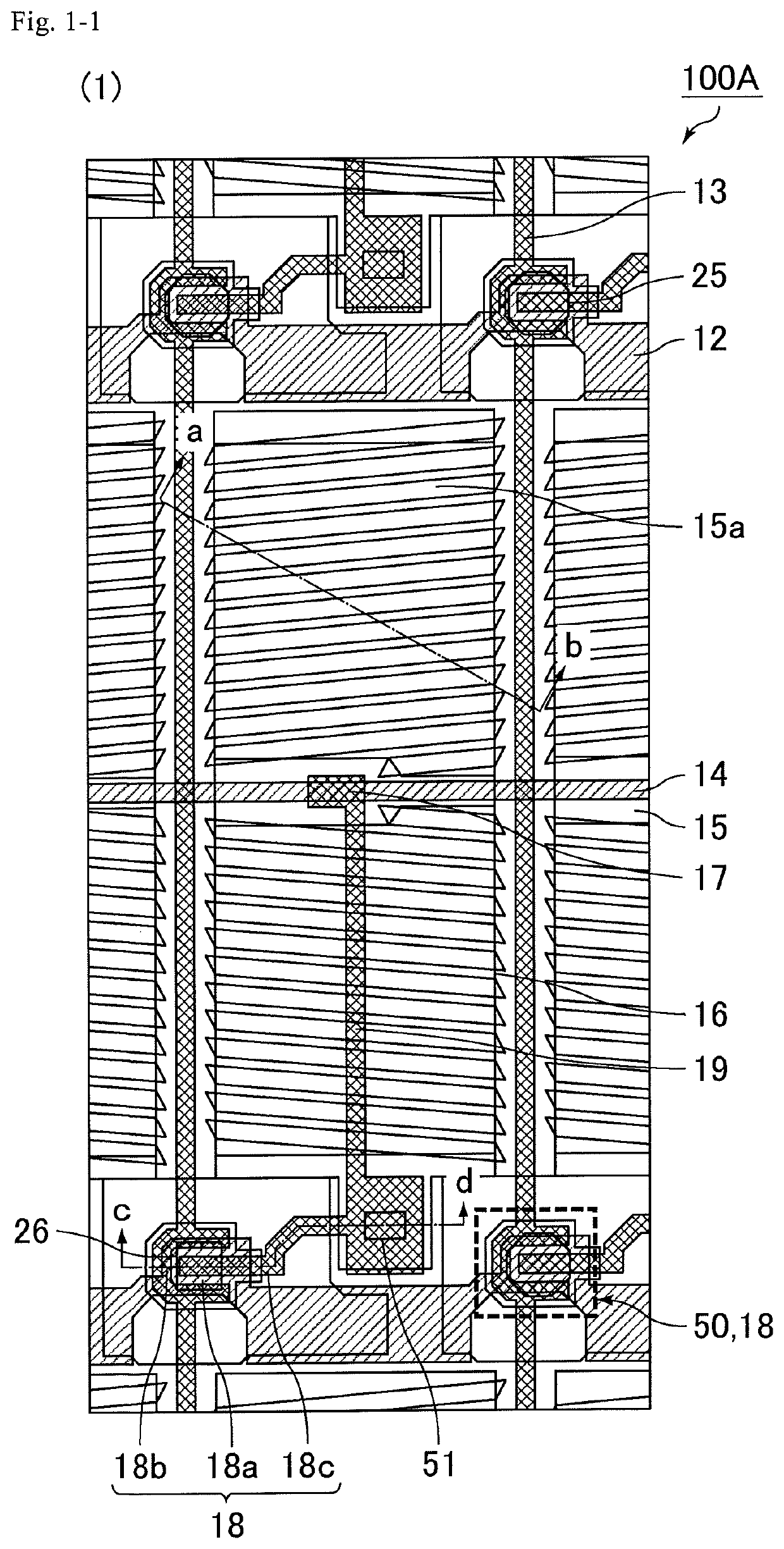
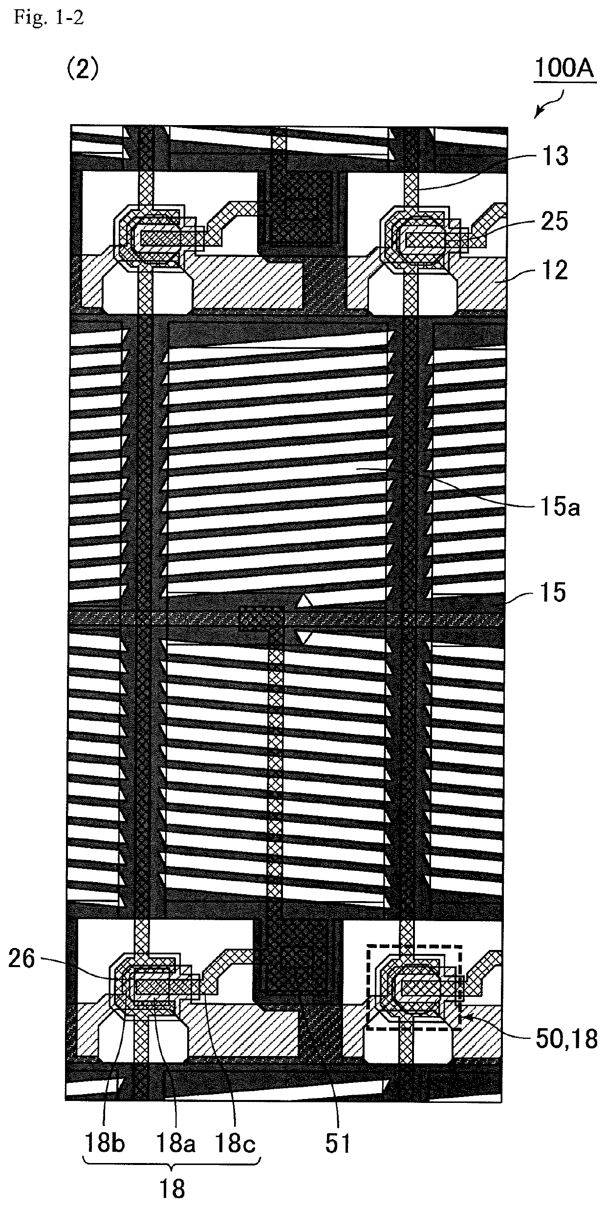
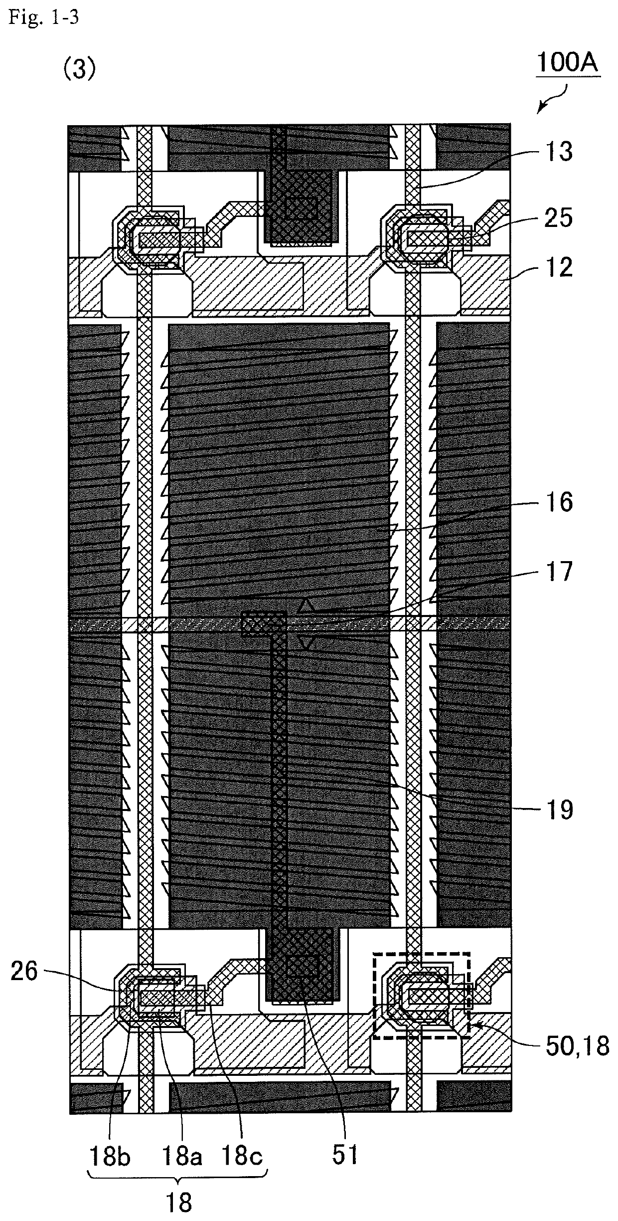
[0076]A liquid crystal display device of Embodiment 1 is described with reference to FIG. 1-1 to FIG. 9. FIG. 1-1 is a schematic plan view of a pixel in a liquid crystal display device of Embodiment 1. FIG. 1-2 is a view of the liquid crystal display device of Embodiment 1 with a common electrode highlighted. FIG. 1-3 is a view of the liquid crystal display device of Embodiment 1 with pixel electrodes highlighted. FIG. 1-4 is a view of the liquid crystal display device of Embodiment 1 with a black matrix highlighted. FIG. 2 is a schematic cross-sectional view of the liquid crystal display device of Embodiment 1. FIG. 3 is a schematic cross-sectional view of a TFT and a contact hole in the liquid crystal display device of Embodiment 1. FIG. 2 shows a cross section taken along the line a-b shown in FIG. 1-1. FIG. 3 shows a cross section taken along the line c-d shown in FIG. 1-1.
[0077]A liquid crystal display device 100A of Embodiment 1 is a normally black FFS mode liquid crystal disp...
embodiment 2
[0138]A liquid crystal display device 200A of Embodiment 2 has the same configuration as the liquid crystal display device 100A of Embodiment 1 except for the positions of the openings 15a in the common electrode 15 and the positions and structure of the contact holes 51. Hence, three features unique to the present embodiment are mainly described below, and the same features as those in Embodiment 1 are not described.
[0139]A first feature of the liquid crystal display device 200A of Embodiment 2 is described. FIG. 10 is a schematic plan view of a liquid crystal display device of Embodiment 2. In the liquid crystal display device 200A of Embodiment 2, each pixel surrounded by the corresponding scanning lines 12 and the corresponding data lines 13 includes four regions defined by the dotted lines as shown in FIG. 10. In each of the four regions, the openings 15a in the common electrode 15 are oriented in the same direction, and the openings 15a in adjacent regions are oriented in diff...
modified example 1 of embodiment 2
[0152]FIG. 13 is a schematic plan view of a liquid crystal display device of Modified Example 1 of Embodiment 2. The liquid crystal display device 200A of Modified Example 1 of Embodiment 2 includes no drain lead line 19 to connect two contact holes 51. In the liquid crystal display device 200A of Modified Example 1 of Embodiment 2, the counter electrodes 17 are disposed in the same layer as the drain electrodes 18c of the TFTs 18, and the TFTs 18 and the respective counter electrodes 17 are connected via the respective pixel electrodes 16. Thus, the counter electrodes 17 can be disposed separately from the drain electrodes 18c. This can increase the aperture ratio of the liquid crystal display device 200A.
PUM
| Property | Measurement | Unit |
|---|---|---|
| thickness | aaaaa | aaaaa |
| pre-tilt angle | aaaaa | aaaaa |
| pre-tilt angle | aaaaa | aaaaa |
Abstract
Description
Claims
Application Information
 - Generate Ideas
- Intellectual Property
- Life Sciences
- Materials
- Tech Scout
- Unparalleled Data Quality
- Higher Quality Content
- 60% Fewer Hallucinations
Browse by: Latest US Patents, China's latest patents, Technical Efficacy Thesaurus, Application Domain, Technology Topic, Popular Technical Reports.
© 2025 PatSnap. All rights reserved.Legal|Privacy policy|Modern Slavery Act Transparency Statement|Sitemap|About US| Contact US: help@patsnap.com