Optical proximity effect correcting method

A technology of optical proximity effect and pattern, applied in optics, originals for opto-mechanical processing, opto-mechanical equipment, etc., to achieve the effect of improving process margin and reducing deformation amount

Inactive Publication Date: 2004-10-13
UNITED MICROELECTRONICS CORP
View PDF0 Cites 0 Cited by
  • Summary
  • Abstract
  • Description
  • Claims
  • Application Information

AI Technical Summary

Problems solved by technology

However, when the key size of the transfer pattern and the distance between the patterns are reduced to a certain extent, if the method and proportion of the prior art are used to add corner serifs or hammerhead patterns, it is still impossible to effectively avoid the tail end of the pattern. shrink

Method used


Image

  • Optical proximity effect correcting method
  • Optical proximity effect correcting method
  • Optical proximity effect correcting method

Examples


Embodiment Construction

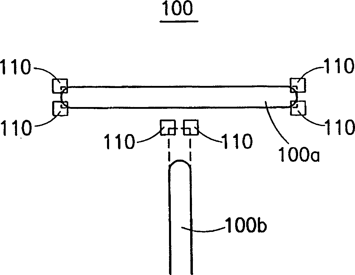
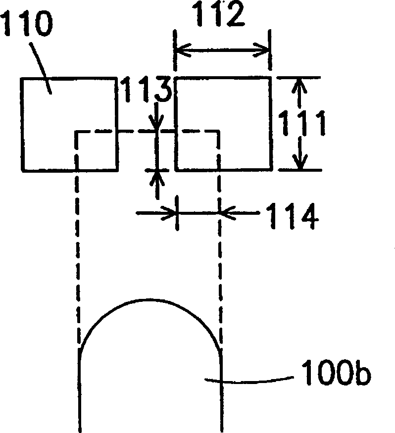
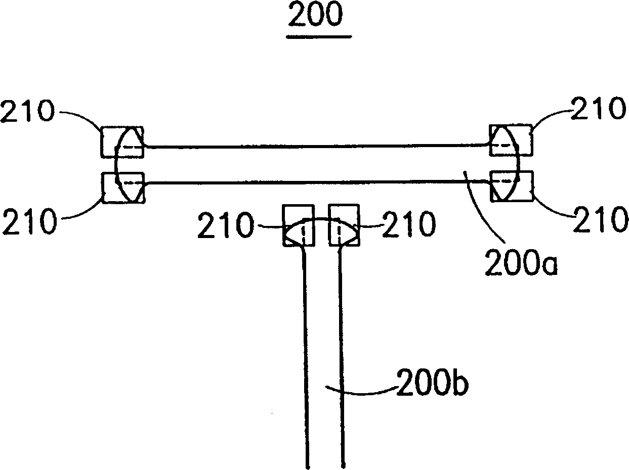
[0029] Generally speaking, the equipment used in the lithographic etching process includes a reticle, also known as a mask, with a pattern on the reticle corresponding to a pattern on a certain layer of an integrated circuit. Typically, the wire mesh consists of a glass plate covered by a defined opaque layer, eg chrome. During exposure, the wire grid is placed between the wafer and the light source. When the light source is incident on the wire grid, the light will pass through the glass layer not covered by the opaque layer and project to a photoresist layer on the wafer. In this way, the pattern on the wire net is transferred to the photoresist layer.

[0030] As mentioned above, due to the refraction or interference of light passing through the mask during exposure, and other factors in the manufacturing process, the transferred pattern is deformed. In order to make the transferred pattern realistic and reduce its deformation, the present invention provides a method for c...


PUM


Abstract

The present invention is optical proximity effect correcting method. Margin line or hammer like pattern is utilized to avoid tail contraction of main pattern and to make the tail of main pattern after exposure approach initial design value in length with tailing end being slightly wider. The length approaching initial design can avoid incomplete contact or breakdown of metal interconnection lines caused by bad aligning. The slightly wider tail increases the technological tolerance of metal interconnection line.

Description

technical field [0001] The present invention relates to an Optical Proximity Correction (OPC) method, in particular to a method for correcting the Optical Proximity Effect suitable for designing and manufacturing a metal interconnection mask. Background technique [0002] Today, with the vigorous development of integrated circuits, the miniaturization and integration of components is an inevitable trend, and it is also an important topic for active development in all walks of life. In the manufacturing process of integrated circuits, the photolithographic etching step becomes an important key to determine the performance of components. With the gradual increase of the integration level, the size of the components is gradually reduced, and the distance between the components must also be reduced, thus causing deviations in the pattern transfer during the lithographic etching step. When the etching is transferred to a wafer, the right-angle part of the pattern is rounded, the...

Claims


Application Information

Patent Timeline
Patent Type & Authority Patents(China)
IPC IPC(8): G03F1/36G03F7/20G03F7/22G03F9/00
Inventor 林金隆
Owner UNITED MICROELECTRONICS CORP
Why Eureka
Try Eureka