
Magnetic tunnel junction structure having an oxidized buffer layer and method of fabricating the same

a tunnel junction and buffer layer technology, applied in the field of magnetic tunnel junction structures, can solve the problems of device failure in the mram device, short circuit between the upper magnetic layer, and technique does have limitations

Inactive Publication Date: 2005-02-17
SAMSUNG ELECTRONICS CO LTD
View PDF3 Cites 17 Cited by
  • Summary
  • Abstract
  • Description
  • Claims
  • Application Information

AI Technical Summary

Benefits of technology

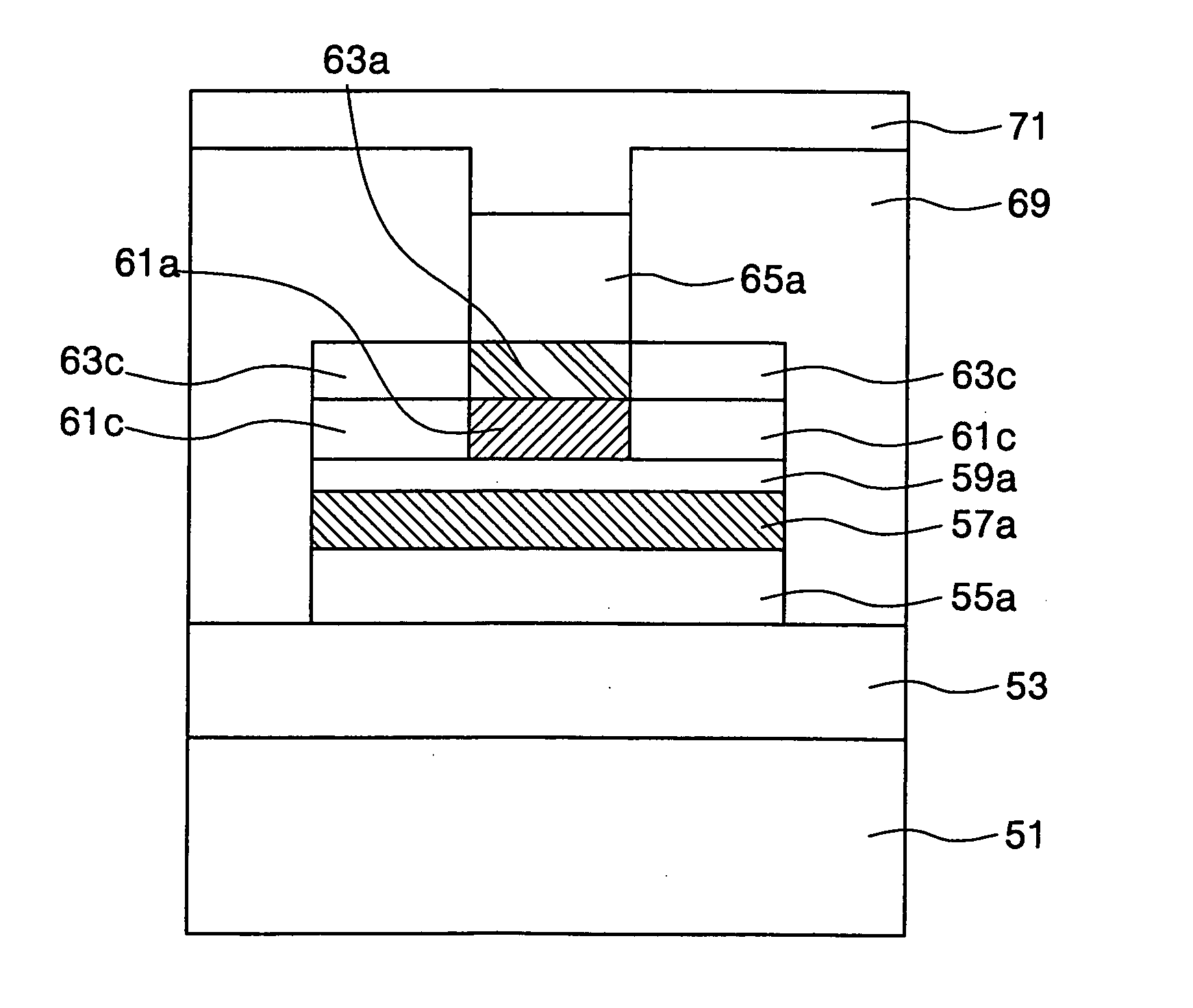
[0022] An exemplary embodiment of the present invention provides an improved magnetic tunnel junction structure that results in a higher process margin resulting from the subsequent ashing process.
[0023] Another feature of the present disclosure provides an improved method of fabricating a magnetic tunnel junction structure that is less likely to result in a short between an upper magnetic layer and a lower magnetic layer.
[0026] The oxidized buffer layer prevents oxygen atoms from deteriorating the upper magnetic layer pattern during a subsequent process.

Problems solved by technology

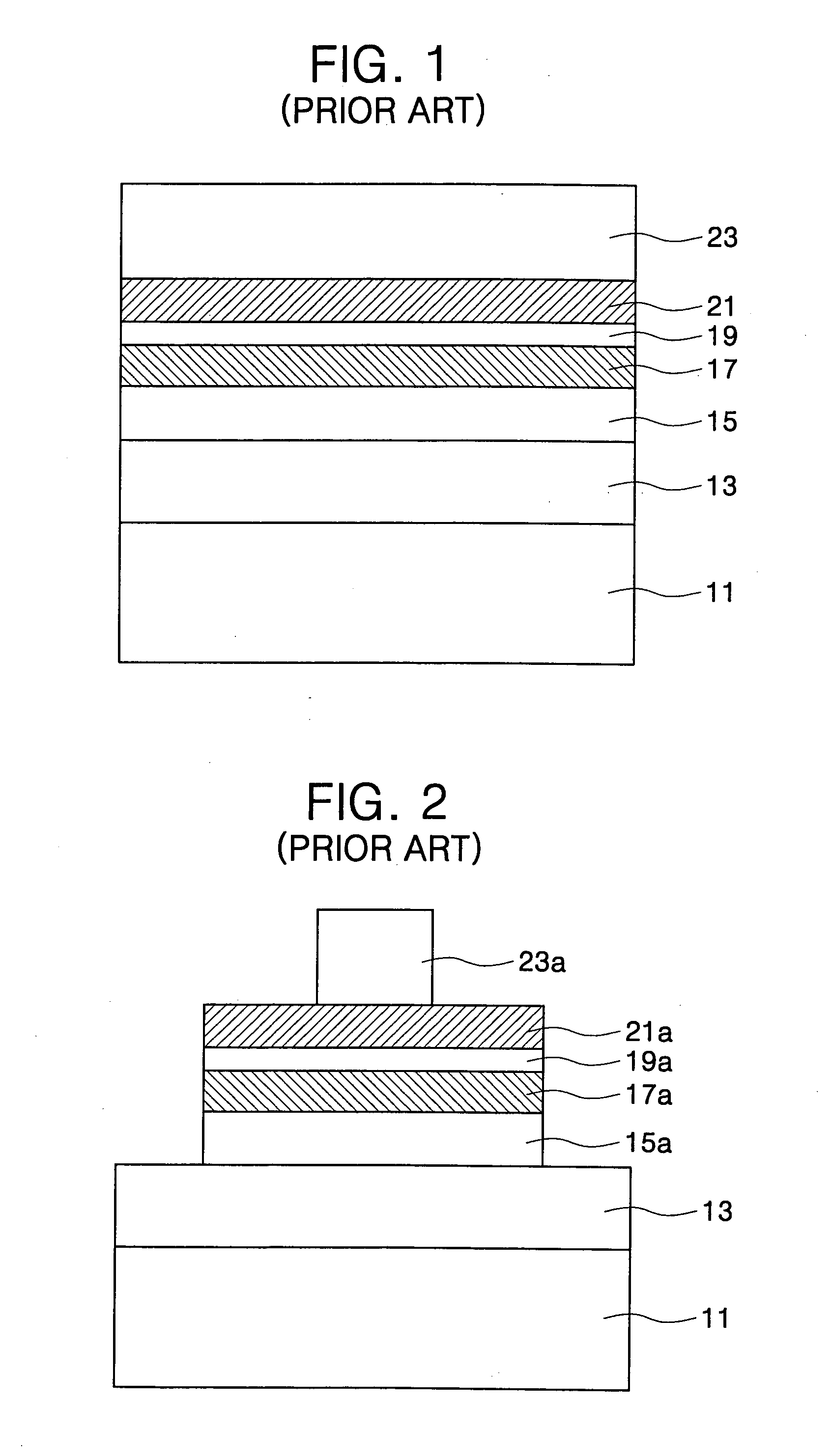
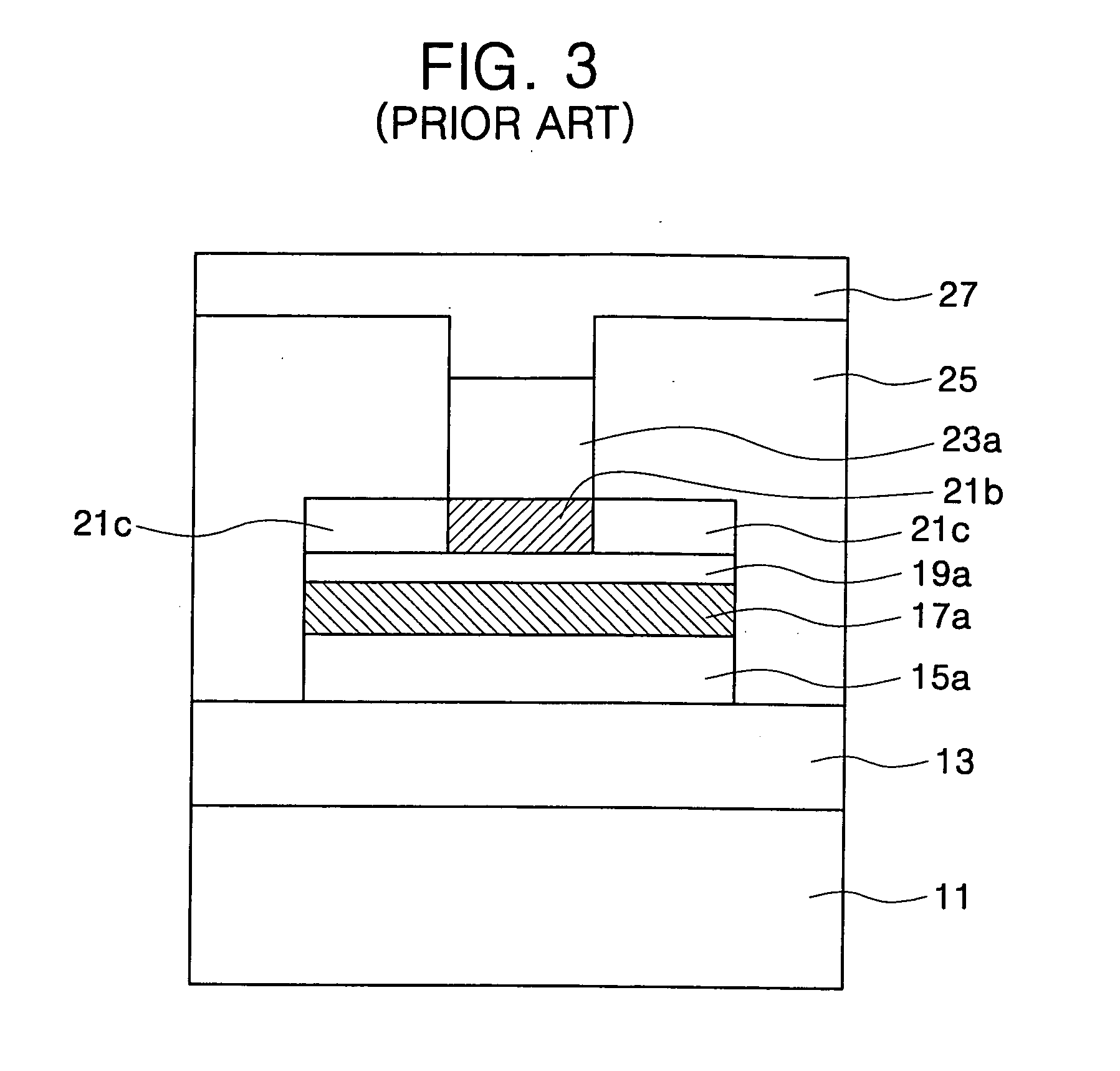
However, while sequentially etching the upper magnetic layer and the lower magnetic layer, etch residues may occur and cause a short circuit between the upper magnetic layer and the lower magnetic layer.
Said short circuit results in a device failure in an MRAM device and must be avoided.
However, this technique does have some limitations.
Therefore, this technique results in an undesirable and restrictive temperature requirement during the oxidation process.
However, ashing is performed at a relatively high temperature that may exceed the aforementioned temperature requirement and thus deteriorate the final upper magnetic layer pattern 21b.
Furthermore, to meet the temperature requirement, the upper insulating layer 25 must be formed using a low temperature process, typically lower than 300° C. However, it is difficult to adequately form the upper insulating layer with a desired high density while using this low temperature process because at the low temperature the upper insulating layer has a tendency to be formed porous.
Accordingly, it is difficult to ensure process margins after the oxidation process and a subsequent ashing process required by this conventional technique.

Method used


Image

  • Magnetic tunnel junction structure having an oxidized buffer layer and method of fabricating the same
  • Magnetic tunnel junction structure having an oxidized buffer layer and method of fabricating the same
  • Magnetic tunnel junction structure having an oxidized buffer layer and method of fabricating the same

Examples


examples

[0054] The magnetoresistances of samples having the MTJ structure fabricated according to the embodiment of the present invention, as described above, in which a buffer layer was employed, and an oxidation process was performed after the buffer layer was exposed was recorded, as was the magnetoresistance of other samples having another MTJ structure fabricated by further etching the buffer layer, and exposing an upper magnetic layer, and performing an oxidation process. The measurement results are summarized as MR ratio (MRR) in Table 1. The buffer layer was formed of Ta with thickness of 100 Å, and the oxidation process was performed using an O2 plasma gas at a temperature of 200° C. for one minute for all samples. Further, the exposed layers, buffer layer or upper magnetic layer, were overetched as shown in Table 1. The magnetoresistances were measured by applying an sensing voltage of 0.4 V. Here, the MRR can be given by Equation 1 as follows, by using Rmin of the tunnel layer pa...


PUM


Abstract

There are provided a magnetic tunnel junction structure and a method of fabricating the same. The magnetic tunnel junction structure includes a lower electrode, a lower magnetic layer pattern and a tunnel layer pattern, which are sequentially formed on the lower electrode. The magnetic tunnel junction structure further includes an upper magnetic layer pattern, a buffer layer pattern, and an upper electrode, which are sequentially formed on a portion of the tunnel layer pattern. The sidewall of the upper magnetic layer pattern is surrounded by an oxidized upper magnetic layer, and the sidewall of the buffer layer pattern is surrounded by an oxidized buffer layer. The depletion of the upper magnetic layer pattern and the lower magnetic layer pattern in the magnetic tunnel junction region can be prevented by the oxidized buffer layer.

Description

CROSS-REFERENCE TO RELATED APPLICATION [0001] This application claims priority from Korean Patent Application No. 2003-55559, filed on Aug. 11, 2003, the disclosure of which is hereby incorporated herein by reference in its entirety. BACKGROUND OF THE INVENTION [0002] 1. Field of the Invention [0003] The present invention relates to a magnetic tunnel junction structure and a method of fabricating the same, and more particularly, to a magnetic tunnel junction structure having an oxidized buffer layer, and a method of fabricating the same. [0004] 2. Description of the Related Art [0005] Semiconductor memory devices for storing information are normally classified into volatile memory devices and non-volatile memory devices. Whereas the volatile memory devices lose stored information therein when a power supply is shut off, the non-volatile memory devices still keep stored information even when a power supply is shut off. Such non-volatile memory devices including flash memory devices, ...

Claims


Application Information

Patent Timeline
Patent Type & Authority Applications(United States)
IPC IPC(8): G11C11/15H01L21/00H10N50/01H10N50/10
CPCH01L43/12H01L43/08H10N50/01H10N50/10G11C11/15
Inventor HA, YOUNG-KILEE, JANG-EUNKIM, HYUN-JOOH, SE-CHUNGBAE, JUN-SOOBAEK, IN-GYU
Owner SAMSUNG ELECTRONICS CO LTD
Learn More