
Self-biased high-adaptability crystal oscillation integrated circuit

A crystal oscillation and integrated circuit technology, applied in power oscillators, electrical components, etc., can solve the problems of reduced phase margin of oscillators, unfavorable oscillators, and no current power consumption control system, and achieve the effect of avoiding current consumption

Inactive Publication Date: 2022-07-15
深圳市万微半导体有限公司
View PDF12 Cites 0 Cited by
  • Summary
  • Abstract
  • Description
  • Claims
  • Application Information

AI Technical Summary

Problems solved by technology

[0004] However, in traditional Pierce oscillators, according to different crystal oscillator manufacturers, the equivalent series resistance ESR at room temperature and pressure can range from 20Kohm to 100Kohm, and even some vacuum-packaged crystal oscillators can range from 20Kohm to 100Kohm. 1Mohm, the ESR with a huge variation range leads to a reduction in the phase margin of the oscillator, which is very unfavorable for the design of the oscillator's peripheral circuit
In addition, for the Internet of Things (IOT) system-on-chip (SOC), which is more and more widely used, in the crystal oscillator as the basic unit of timing, if the timing deviates because the power supply (battery) is exhausted, it is Extremely need to be avoided, and the traditional Pierce oscillator does not have a controllable current power consumption control system, it can only be carried out according to simulation, and due to the deviation of the integrated circuit chip process, the power consumption consistency between chips is also very poor

Method used


Image

  • Self-biased high-adaptability crystal oscillation integrated circuit
  • Self-biased high-adaptability crystal oscillation integrated circuit
  • Self-biased high-adaptability crystal oscillation integrated circuit

Examples


Embodiment 1

[0068] like Figure 7 shown in Figure 4 On the basis of the shown embodiment, a two-stage differential comparator circuit is added. The specific circuit structure is:

[0069] One end of the crystal oscillator X is connected to one end of the second resistor R2 and the gate of the sixth MOS transistor M6, and the other end of the second resistor R2 is connected to the third capacitor C3, the gate of the second MOS transistor M2, and the gate of the fifth MOS transistor M5. The gate is connected, the source of the fifth MOS transistor M5 and the source of the sixth MOS transistor M6 are connected to the drain of the tenth MOS transistor M10, and the drain of the fifth MOS transistor M5 is connected to the drain of the seventh MOS transistor M7 , the gate of the seventh MOS transistor M7 and the gate of the eighth MOS transistor M8 are connected, the drain of the eighth MOS transistor M8 is connected to the drain of the sixth MOS transistor M6 and the gate of the ninth MOS tr...

Embodiment 2

[0075] like Figure 8 As shown, this embodiment uses a PMOS transistor as the input MOS pair of transistors, which is the same as the Figure 7 The circuit shown is only different in the second-level differential comparator circuit. The specific circuit structure of this part is:

[0076] One end of the crystal oscillator X is connected to one end of the second resistor R2 and the gate of the fifth MOS transistor M5, and the other end of the second resistor R2 is connected to the third capacitor C3, the gate of the second MOS transistor M2, and the gate of the sixth MOS transistor M6. gate connection,

[0077]The source of the fifth MOS transistor M5 and the source of the sixth MOS transistor M6 are both connected to the drain of the tenth MOS transistor M10, and the drain of the fifth MOS transistor M5 is connected to the drain of the seventh MOS transistor M7 and the seventh MOS transistor M10. The gate of the transistor M7 and the gate of the eighth MOS transistor M8 are ...

Embodiment 3

[0083] like Figure 9 As shown, this embodiment uses a PMOS tube as the input pair tube and current mirror of the self-biased current source circuit, which is the same as the Figure 7 The circuit shown differs only in the crystal oscillator circuit and the self-biased current source circuit. The specific circuit structure of this part is:

[0084] One end of the crystal oscillator X is connected to the drain of the first MOS transistor M1, the drain of the fourth MOS transistor, and one end of the first capacitor C1, and the other end of the crystal oscillator X is connected to one end of the second capacitor C2, one end of the second resistor R2, The gate of the first MOS transistor M1 and the gate of the sixth MOS transistor M6 are connected, two ends of the nonlinear MOS transistor are respectively connected to two ends of the crystal oscillator X, and the other end of the second resistor R2 is connected to one end of the third capacitor C3, The gate of the second MOS tr...


PUM


Abstract

The invention discloses a self-biased high-adaptability crystal oscillation integrated circuit in the technical field of integrated circuit design, which comprises a crystal oscillation circuit and a self-biased current source circuit, the crystal oscillation circuit is used for generating a source signal of crystal oscillation, the self-biased current source circuit is connected with the output end of the crystal oscillation circuit, and the self-biased current source circuit is connected with the output end of the crystal oscillation circuit. The self-bias current source circuit is used for carrying out nonlinear amplification on a source signal of crystal oscillation and comprises a first resistor, and the first resistor is used for generating bias current and controlling overall power consumption. The large-range distribution of the equivalent series resistors of the crystal oscillator is controlled, so that the phase margin of the system circuit is within an acceptable range, and meanwhile, through the application of the self-bias current source circuit, an external bias circuit and bias voltage can be prevented from being not needed, so that the current consumption of another bias circuit module is avoided, and the service life of the system circuit is prolonged. The ultra-low power consumption working state of the system can be realized.

Description

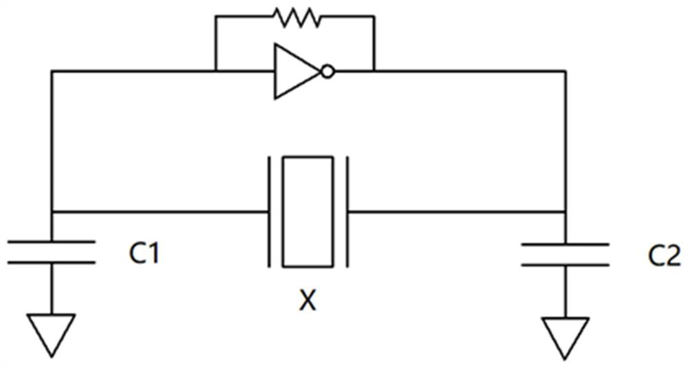
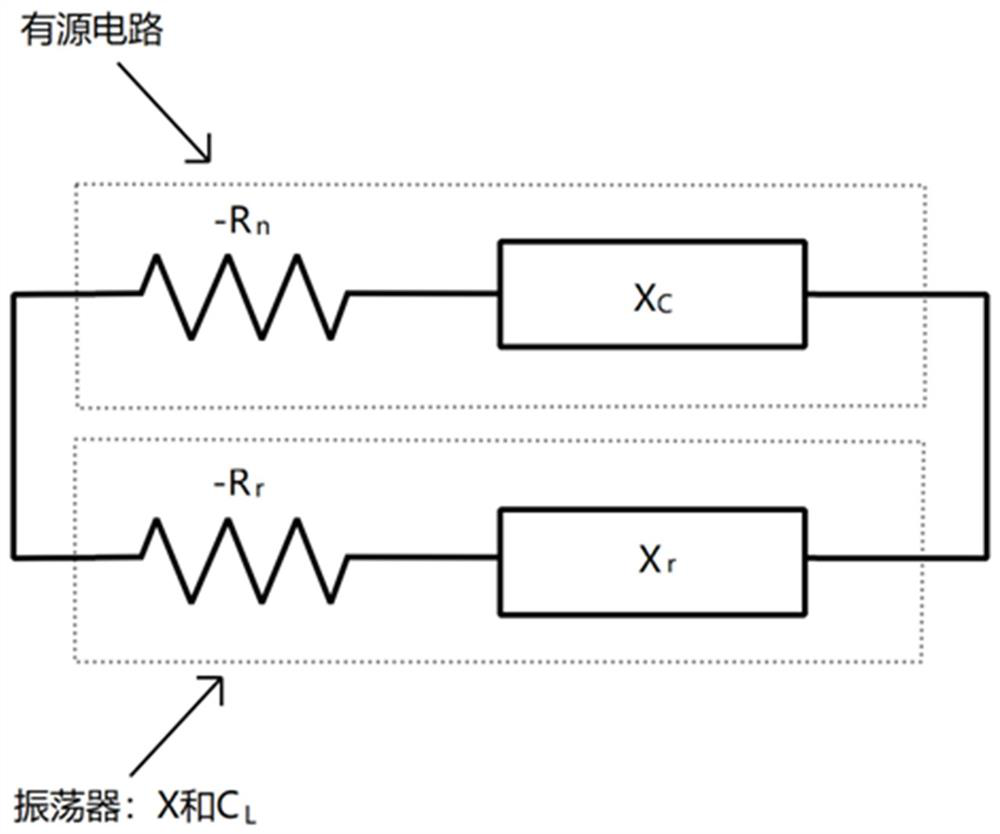
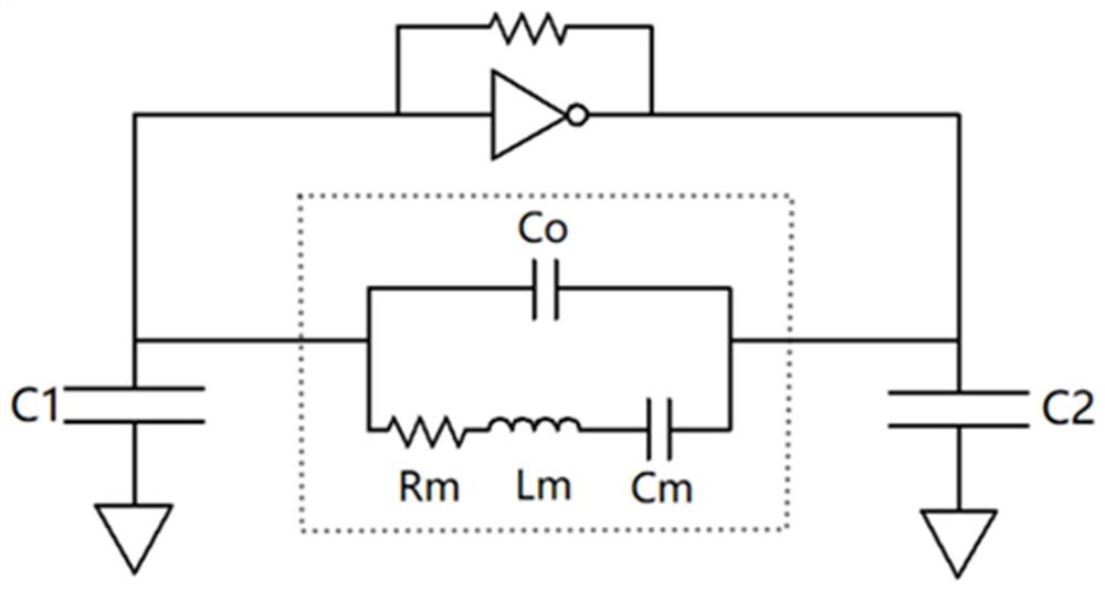
technical field [0001] The present invention relates to the technical field of integrated circuit design, in particular to a self-biased crystal oscillator integrated circuit with high adaptability. Background technique [0002] In modern electronic systems, crystal oscillator circuits are used more and more widely in integrated circuit design as clock generators. Among them, the traditional Pierce oscillator is widely used in integrated circuits including SOC. For example, the Chinese invention patent with the application number 201210559927.X and the Chinese invention patent with the application number 200910152407.5 all use the Pierce oscillator as the clock Signal generator. [0003] like figure 1 As shown, in a traditional Pierce oscillator, the oscillator loop consists of an inverting amplifier, a feedback resistor (usually inside the chip), and a crystal oscillator XTAL (X) and an external load capacitor (C 1 and C 2 ) composed of an accurate phase-shift circuit. ...

Claims


Application Information

Patent Timeline
Patent Type & Authority Applications(China)
IPC IPC(8): H03B5/36
CPCH03B5/364
Inventor 熊力嘉刘磊
Owner 深圳市万微半导体有限公司
Learn More