Modification method of full-suede perovskite/crystalline silicon laminated solar cell
A solar cell and perovskite technology, applied in the field of solar cells, can solve the problems of poor repeatability of the perovskite polycrystalline film process, inability to form intermediate complexes, and uncontrollable crystallization process of the perovskite polycrystalline film. The effect of low difficulty in operation process and simple method
- Summary
- Abstract
- Description
- Claims
- Application Information
AI Technical Summary
Problems solved by technology
Method used
Image
Examples
Embodiment 1
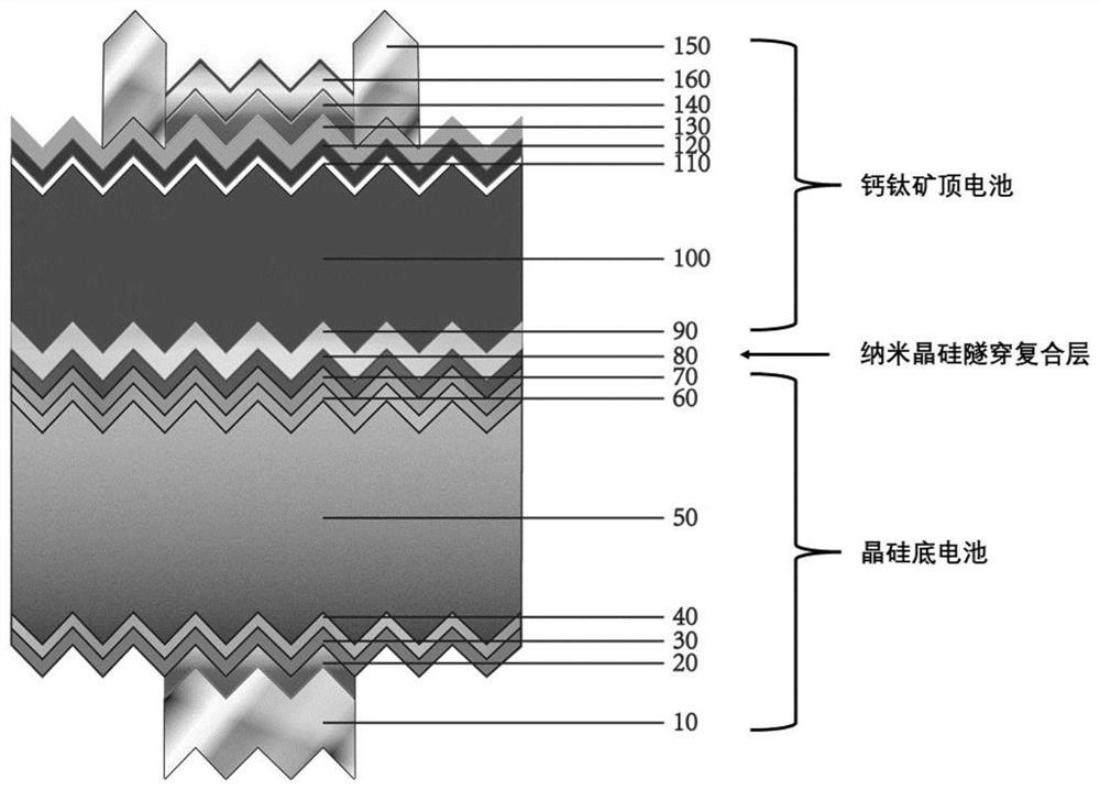
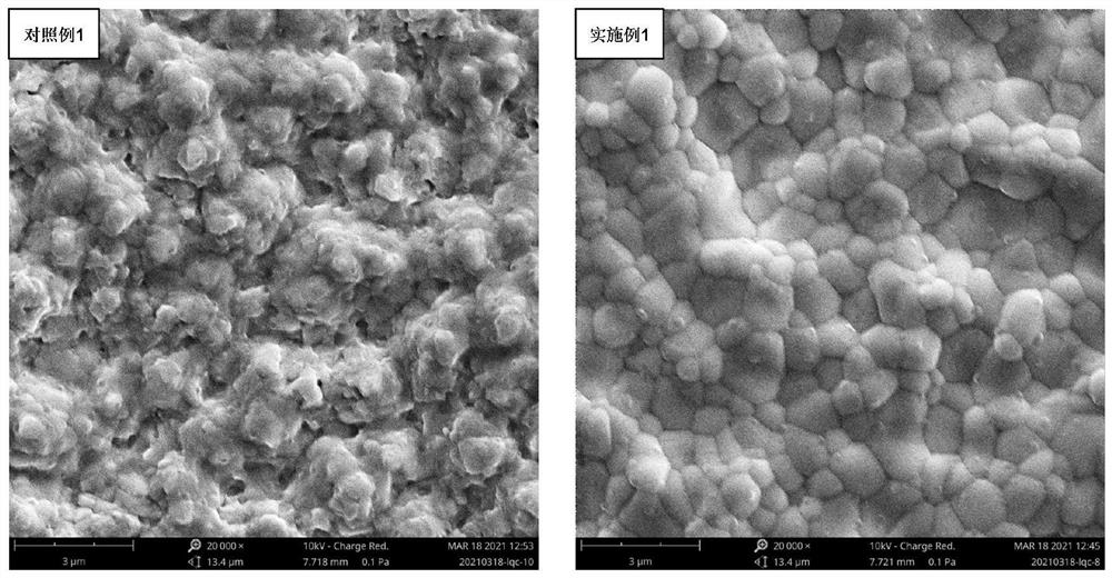
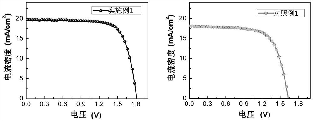
[0031] An embodiment of a method for simultaneously improving the open circuit voltage and stability of a full-textured perovskite / crystalline silicon tandem solar cell, comprising the following steps:
[0032] (1) Select a commercial double-sided textured heterocrystalline silicon cell with no indium tin oxide transparent electrode deposited on the n-type amorphous silicon surface, and use it as the bottom cell of the tandem solar cell. 15nm nanocrystalline silicon was deposited on the crystalline silicon by plasma enhanced chemical vapor deposition equipment as a tunneling composite layer.
[0033] (2) A hole transport layer spiro-TTB with a thickness of 25 nm was deposited on the nanocrystalline silicon as the tunneling composite layer at an evaporation rate of 0.02 nanometers per second in a thermal evaporation vacuum deposition equipment; The first step of preparing the perovskite light absorbing layer by the step method: co-evaporating lead iodide and cesium bromide usin...
Embodiment 2
[0047] An embodiment of a method for simultaneously improving the open circuit voltage and stability of a full-textured perovskite / crystalline silicon tandem solar cell, comprising the following steps:
[0048] (1) Select a commercial double-sided textured heterocrystalline silicon cell with no indium tin oxide transparent electrode deposited on the n-type amorphous silicon surface, and use it as the bottom cell of the tandem solar cell. 15nm nanocrystalline silicon was deposited on the crystalline silicon by plasma enhanced chemical vapor deposition equipment as a tunneling composite layer.
[0049] (2) A hole transport layer spiro-TTB with a thickness of 25 nm was deposited on the nanocrystalline silicon as the tunneling composite layer at an evaporation rate of 0.02 nanometers per second in a thermal evaporation vacuum deposition equipment; The first step of preparing the perovskite light absorbing layer by step method: co-evaporating lead iodide and cesium bromide using th...
PUM
 Abstract
Description
Claims
Application Information
 - R&D Engineer
- R&D Manager
- IP Professional
- Industry Leading Data Capabilities
- Powerful AI technology
- Patent DNA Extraction
Browse by: Latest US Patents, China's latest patents, Technical Efficacy Thesaurus, Application Domain, Technology Topic, Popular Technical Reports.
© 2024 PatSnap. All rights reserved.Legal|Privacy policy|Modern Slavery Act Transparency Statement|Sitemap|About US| Contact US: help@patsnap.com


