
Filter chip and processing method thereof

A processing method and filter technology, applied in the field of filters, can solve problems such as damage to resonators in chips, impact on filter performance, and easy damage to resonators, so as to improve resonance energy efficiency, strong anti-interference effect, and reduce impact Effect

Pending Publication Date: 2022-05-10
SHANGHAI PINGSHENG MICRO CORP
View PDF0 Cites 0 Cited by
  • Summary
  • Abstract
  • Description
  • Claims
  • Application Information

AI Technical Summary

Problems solved by technology

[0002] The resonance area of ​​the low, medium and high frequency filter is covered with a silicon dioxide protective layer. The advantage is that it helps to protect the resonator from external force damage and environmental pollution; the disadvantage is that it has a certain impact on the performance of the filter. Compared with the medium and low frequency filter , the high-frequency filter covering the protective layer has a great influence on the performance
[0003] In the traditional bumping process, the flux brushing and ball planting stencil will be attached to the surface of the filter wafer. When there are foreign objects or scratches on the two stencils during the process of brushing and ball planting, it is easy to cause internal resonance in the chip. organ damage
Resonators are highly susceptible to damage when there is no protective silica layer in the resonator area

Method used


Image

  • Filter chip and processing method thereof
  • Filter chip and processing method thereof
  • Filter chip and processing method thereof

Examples


Embodiment 1

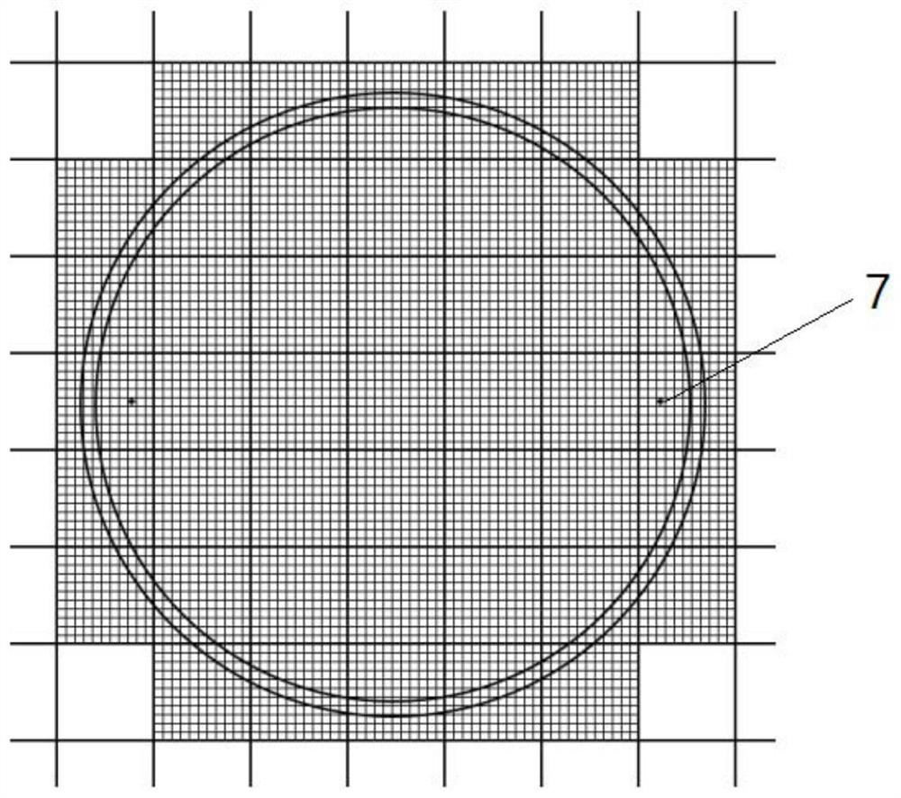
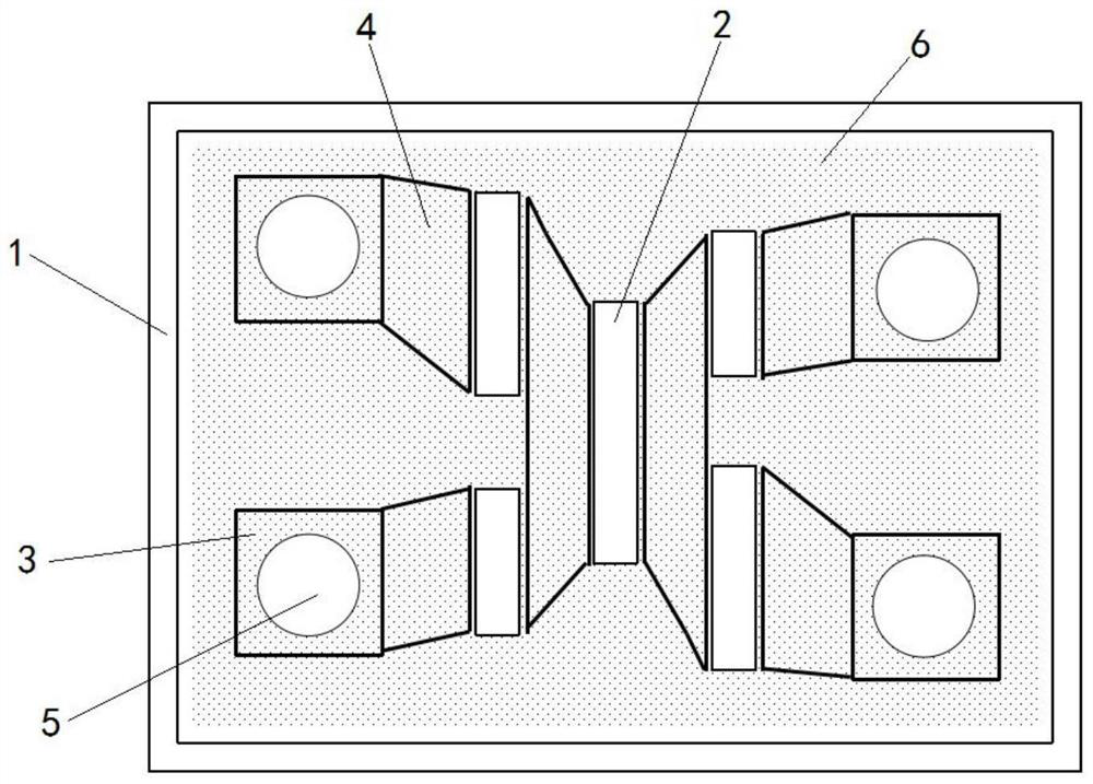
[0032] like Figure 1~2 As shown, a filter chip includes a wafer, and an effective area of ​​the chip is provided on the wafer; a scribing line 1 is provided outside the effective area of ​​the chip; a resonator 2 and a pad 3 are provided in the effective area of ​​the chip; The pad 3 is connected to the resonator 2 through the metal line 4; solder balls 5 are planted in the ball planting area of ​​the pad 3;

Embodiment 2

[0034] A processing method for a filter chip, comprising the following steps:

[0035] Step 1: Design and process the wafer of the filter; the wafer structure is as Figure 1~2 As shown, determine the alignment coordinates 7; process the scribe line on the wafer; install resonators, metal lines and pads in the effective area of ​​the chip; covered with a silicon dioxide protective layer;

[0036] Step 2: Implanting solder balls 5 on the pads 3 by means of bumping processing.

[0037] Before the bumping process, it is necessary to design the photoresist mask and the stencil for brushing and planting balls.

[0038] (1) Design and process the photoresist mask plate: open a window at the position corresponding to the photoresist mask plate and the ball planting area of ​​the pad;

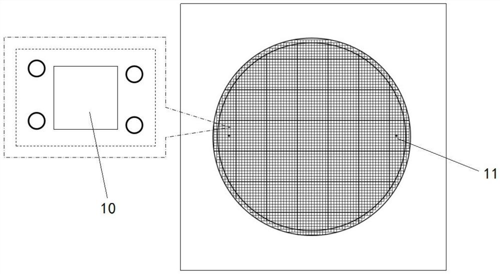
[0039] (2) Design and process brushing and ball planting steel mesh 8, such as Figure 3-5 As shown; the brushing and ball planting steel mesh 8 is provided with an opening 9 corresponding to the b...


PUM

PropertyMeasurementUnit
thicknessaaaaaaaaaa
thicknessaaaaaaaaaa
thicknessaaaaaaaaaa

Abstract

The invention provides a filter chip and a processing method thereof, and relates to the technical field of filters. The filter chip comprises a wafer, and a chip effective area is arranged on the wafer. Scribing channels are arranged outside the chip effective area; a resonator and a bonding pad are arranged in the effective area of the chip; the bonding pad is connected with the resonator through a metal line; solder balls are planted in the ball planting area of the bonding pad; and a silicon dioxide protection layer covers the surface of the effective area of the chip except the solder balls and the resonators. The resonator area of the filter chip is not covered with a silicon dioxide protection layer, so that the flexible input and output and high-frequency conversion functions of the resonator are kept; the influence of the silicon dioxide protection layer on the performance of the filter chip is reduced, the resonance energy efficiency of the filter is improved, and particularly, the anti-interference effect of the high-frequency filter is stronger. The semi-etched cavity corresponding to the resonator on the wafer is arranged on the scaling powder brush coating and ball mounting steel mesh, so that the resonator is prevented from being damaged in the machining process.

Description

technical field [0001] The invention relates to the technical field of filters, in particular to a filter chip and a processing method thereof. Background technique [0002] The resonance area of ​​the low, medium and high frequency filter is covered with a silicon dioxide protective layer. The advantage is that it helps to protect the resonator from external force damage and environmental pollution; the disadvantage is that it has a certain impact on the performance of the filter. Compared with the medium and low frequency filter , the protective layer covered by the high-frequency filter has a greater impact on performance. [0003] In the traditional bumping process, the flux brushing and ball planting stencil will be attached to the surface of the filter wafer. When there are foreign objects or scratches on the two stencils during the process of brushing and ball planting, it is easy to cause internal resonance in the chip. device damaged. When there is no protective l...

Claims


Application Information

Patent Timeline
Patent Type & Authority Applications(China)
IPC IPC(8): H03H3/02H03H9/46
CPCH03H3/02H03H9/46
Inventor 吴现伟汪洋
Owner SHANGHAI PINGSHENG MICRO CORP
Learn More