


Quick Research
Generate reliable direction feasibility study reports for your R&D in just a few steps.

Technical Q&A
Discover and master advanced knowledge NOW. Basics, ideas, possibilities, all at once.

Find Solutions
As an expert in R&D theories, this can generate solutions to your technical problems instantly.

Evaluate Feasibility
Analyze your overall solution with one click, know your potential R&D risks in advance.

Monitor Landscape
Get weekly tech updates, stay abreast of the latest tech innovations and key insights.
Programmable ultra-narrow power pulse sharpening circuit and method
A power pulse, sharpening circuit technology, applied in pulse shaping and other directions, to achieve the effect of improving applicability, improving overall processing efficiency, and reducing parasitic inductance
- Summary
- Abstract
- Description
- Claims
- Application Information
AI Technical Summary
Problems solved by technology
Method used
Image


Examples
Embodiment 1
[0057] In an exemplary embodiment, a programmable ultra-narrow power pulse sharpening circuit is provided, and the sharpening circuit includes a DC power supply, a first capacitor C1, a first half-bridge circuit, a second half-bridge circuit and Load, the first half-bridge circuit and the second half-bridge circuit are cascaded to output ultra-narrow power pulses; the duty cycle dead zones of the first half-bridge circuit and the second half-bridge circuit are the same;
[0058] The first half-bridge circuit includes at least a pair of transistors with complementary control signals, and the second half-bridge circuit includes at least a pair of transistors with complementary control signals; the control signal of the second half-bridge circuit is higher than that of the first half-bridge circuit. The control signal of the bridge circuit is delayed so that the sharpening circuit discharges quickly.
[0059] Specifically, by cascading the first half-bridge circuit and the second...
Embodiment 2
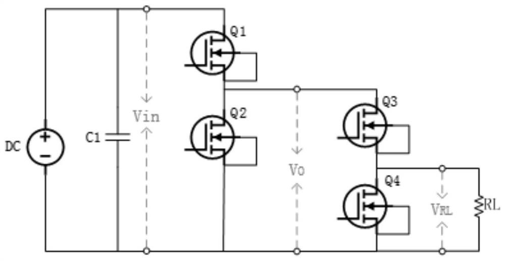
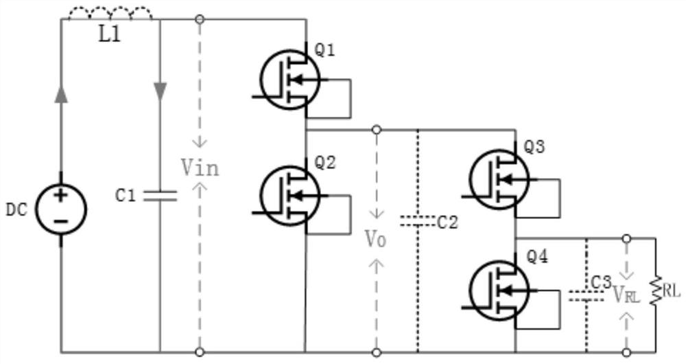
[0067] Based on Embodiment 1, a programmable ultra-narrow power pulse sharpening circuit is provided, such as figure 1 As shown, the first half-bridge circuit includes a first transistor Q1 and a second transistor Q2, and the second half-bridge circuit includes a third transistor Q3 and a fourth transistor Q4, and RL in the figure represents a load.
[0068] One end of the first capacitor C1 is connected to the positive pole of the direct current power supply, the other end of the first capacitor C1 is connected to the negative pole of the direct current power supply DC, and the drain of the first transistor Q1 is connected to the first On the common connection point between a capacitor C1 and the positive pole of the direct current power supply DC, the source of the first transistor Q1 is connected to the drain of the second transistor Q2, and the source of the second transistor Q2 is connected to the On the common connection point of the first capacitor C1 and the DC negativ...
Embodiment 3
[0082] Gallium nitride (GaN) has been regarded as a next-generation semiconductor material for power electronic devices with high efficiency and high power density. Compared with silicon Si materials, the high-frequency switching characteristics of GaN power devices allow them to be used as small on-board passive components, thereby reducing parasitic losses and costs. Although discrete GaN power devices have demonstrated excellent characteristics, most peripheral control / drive modules are composed of these discrete GaN devices using Si technology. In order to verify the rationality of the theoretical scheme design, the simulation circuit model built by the spice simulation model of GaN devices using LTspice simulation software is as follows: Figure 8 shown.
[0083] Wherein, assume that the load is a pure resistive load 50Ω to verify the width of the pulse output of the circuit of the present invention, as Figure 9 As shown, the gate-source control signals of four switchi...
PUM
 Abstract
Description
Claims
Application Information
 - R&D Engineer
- R&D Manager
- IP Professional
- Industry Leading Data Capabilities
- Powerful AI technology
- Patent DNA Extraction
Browse by: Latest US Patents, China's latest patents, Technical Efficacy Thesaurus, Application Domain, Technology Topic, Popular Technical Reports.
© 2024 PatSnap. All rights reserved.Legal|Privacy policy|Modern Slavery Act Transparency Statement|Sitemap|About US| Contact US: help@patsnap.com