Method for manufacturing circuit board by using laser to process an electroplating hole, bonding pad plating resistance and conductive pattern

A conductive pattern, laser processing technology, applied in the direction of assembling printed circuits with electrical components, removing conductive materials by light, printing circuits, etc., to achieve the effects of fewer steps, lower costs, and shorter manufacturing processes

Pending Publication Date: 2021-11-26
德中(天津)技术发展股份有限公司
View PDF8 Cites 0 Cited by
  • Summary
  • Abstract
  • Description
  • Claims
  • Application Information

AI Technical Summary

Problems solved by technology

[0017] Aiming at the deficiency that the existing technology cannot only electroplate thickened holes, the present invention has developed a new manufacturing method, and the technical scheme of the present invention is as follows:

Method used


Image

  • Method for manufacturing circuit board by using laser to process an electroplating hole, bonding pad plating resistance and conductive pattern
  • Method for manufacturing circuit board by using laser to process an electroplating hole, bonding pad plating resistance and conductive pattern
  • Method for manufacturing circuit board by using laser to process an electroplating hole, bonding pad plating resistance and conductive pattern

Examples


Embodiment 1

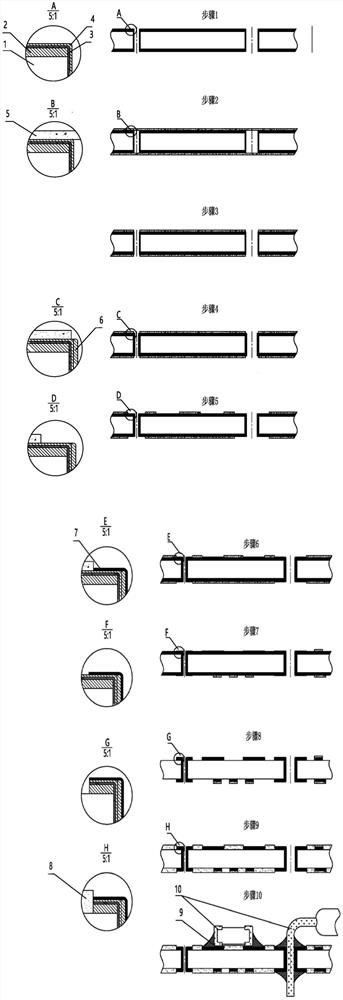
[0084] Copper-clad laminates are commonly used as the basic material to make circuit boards in the electronics industry. The copper-clad laminates include an insulating substrate 1 and a copper-clad laminate copper layer 2 .

[0085] This embodiment takes a double-sided printed circuit board as an example, and the specific processing steps are as follows:

[0086] (1) The circuit board base material copper clad laminate includes an insulating substrate 1 and a copper clad laminate 2. The copper clad laminate is drilled, and the initial conductive layer 3 is deposited on the product in process of the double-sided circuit board that has been drilled, and the copper is electroplated to The thickness can withstand subsequent processes to form electroplated thin copper 4 .

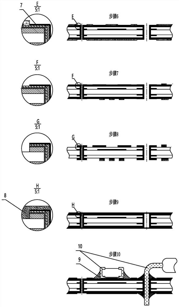
[0087] The purpose of making thin copper on the initial conductive layer is to increase the reliability of the manufacturing process, and its thickness should reach the lower limit to ensure the reliability of ...

Embodiment 2

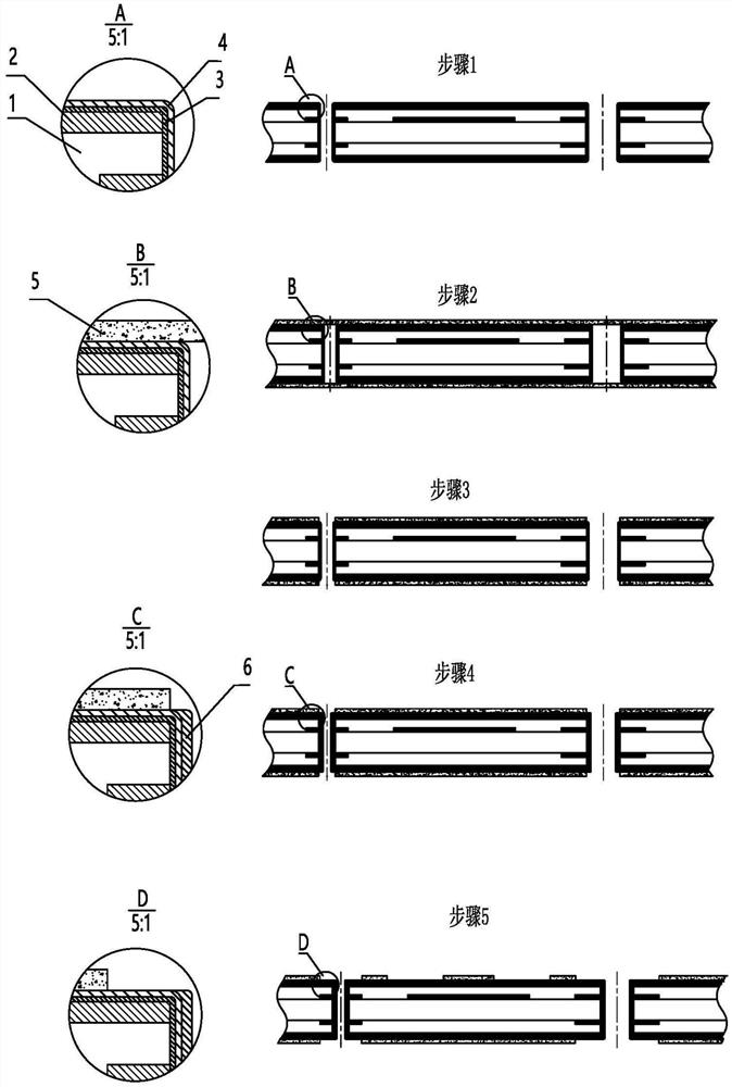
[0121] Copper-clad laminates are commonly used as the basic material to make circuit boards in the electronics industry. The copper-clad laminates include an insulating substrate 1 and a copper-clad laminate copper layer 2 .

[0122] In this embodiment, a four-layer circuit board whose inner circuit has been fabricated is taken as an example, and the specific processing steps are as follows:

[0123] (1) The circuit board base material copper-clad laminate includes an insulating substrate 1 and a copper-clad laminate copper layer 2. The drilled copper-clad laminate is completed, and the initial conductive layer 3 is deposited on the finished product of the four-layer circuit board that has been drilled, and copper is electroplated to The thickness can withstand subsequent processes, forming electroplated thin copper 4;

[0124] The purpose of making thin copper on the initial conductive layer is to increase the reliability of the manufacturing process, and its thickness should...


PUM

PropertyMeasurementUnit
Thicknessaaaaaaaaaa
Thicknessaaaaaaaaaa
Thicknessaaaaaaaaaa

Abstract

The invention relates to a method for manufacturing a circuit board by using laser to process an electroplating hole, a bonding pad plating resistance and a conductive pattern, which comprises the following steps of: drilling, depositing a thin metal layer on the hole and a board surface, pasting a non-photosensitive masking film, removing the masking layer covering the hole wall by laser to expose the hole wall, only electroplating and thickening a conductive layer in the hole, removing the masking layer on the bonding pad area by laser, and exposing the copper surface of the bonding pad; electroplating a metal resist on the hole wall and the bonding pad, coating a non-photosensitive solder resist on a non-circuit area by using a laser-guided pattern, manufacturing a solder resist pattern by using laser on an assembly site, and carrying out cleaning and weldability treatment on the surface of a welding area. The manufacturing process of the circuit board can be integrally optimized and shortened, a non-photosensitive material is used as an anti-electroplating material, only the conductive layer in the hole is electroplated and thickened, only the weldable metal is electroplated on the hole wall and the bonding pad, and the electroplating hole, the hole, the bonding pad pattern and the conductive pattern are manufactured by laser, so that a finer circuit board can be manufactured. The method is suitable for large-scale production of various circuit boards or manufacturing of circuit board samples and small-scale multi-variety products.

Description

technical field [0001] The invention relates to a method for manufacturing circuit boards by laser processing electroplated holes, anti-plating pads and conductive patterns. Non-photosensitive materials are used as masking films to be directly and selectively removed. Only electroplated holes, only electroplated holes and pads belong to circuits. Board making technology field. Background technique [0002] The invention uses laser direct material removal technology to manufacture circuit boards, can only electroplate holes, only electroplate holes and pads, and directly manufacture conductive patterns without pattern transfer process. [0003] The manufacturing process is as follows: Deposit the initial conductive layer on the finished product of the double-sided and multi-layer circuit board that has been drilled, electroless plating or electroplating thin copper → paste anti-plating masking film → pattern the plating hole wall, laser removal The anti-plating masking film ...

Claims


Application Information

Patent Timeline
IPC IPC(8): H05K3/00H05K3/02H05K3/28H05K3/34C25D5/02
CPCH05K3/0026H05K3/027H05K3/282H05K3/34C25D5/022
Inventor 胡宏宇宋金月
Owner 德中(天津)技术发展股份有限公司
Why Eureka
Try Eureka