


Quick Research
Generate reliable direction feasibility study reports for your R&D in just a few steps.

Technical Q&A
Discover and master advanced knowledge NOW. Basics, ideas, possibilities, all at once.

Find Solutions
As an expert in R&D theories, this can generate solutions to your technical problems instantly.

Evaluate Feasibility
Analyze your overall solution with one click, know your potential R&D risks in advance.

Monitor Landscape
Get weekly tech updates, stay abreast of the latest tech innovations and key insights.
Double-sided antireflection film without reducing transmittance of 940-nanometer waveband and preparation method thereof
A transmittance and anti-reflection technology, applied in optics, instruments, optical components, etc., can solve the problems of decreased transmittance, affecting ToF imaging quality, etc., to improve yield, excellent scratch resistance, and reduce costs. Effect
- Summary
- Abstract
- Description
- Claims
- Application Information
AI Technical Summary
Problems solved by technology
Method used
Image

Examples
Embodiment 1
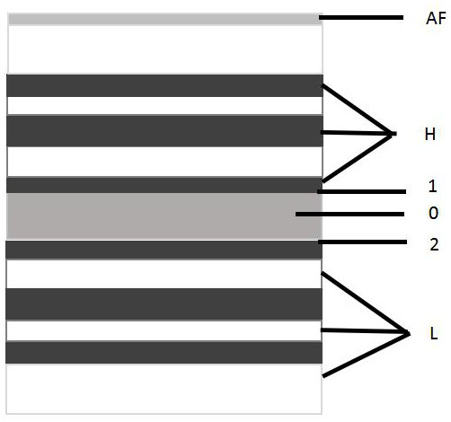
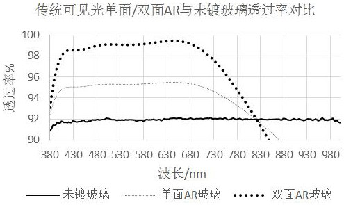
[0054] A traditional double-sided anti-reflection film for improving the transmittance of 420-680nm visible light band to 97.5% or above includes a substrate, a first surface AR, a first surface AF, and a second surface AR.
[0055] In this embodiment, the base material is optical glass whose refractive index at 550 nm is 1.5.
[0056] The first surface and the second surface AR are formed by alternately stacking high and low refractive index materials, the high refractive index niobium oxide; the low refractive index material is silicon oxide.
[0057] The number of AR film layers on the first surface is 6 layers.
[0058] The total thickness of the first surface AR is 254 nm.
[0059] The film structure is Glass / Nb 2 o 5 / SiO 2 / Nb 2 o 5 / SiO 2 / Nb 2 o 5 / SiO 2 / AF / Air, the film thickness of each layer is Glass / 13.94 nm / 33.14 nm / 70.58 nm / 1.75nm / 47.11 nm / 87.45 nm / AF / Air. (The group coefficients of silicon oxide and niobium oxide are both 1)
[0060] The number of ...
Embodiment 2
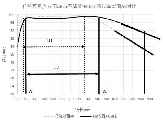
[0066] A double-sided anti-reflection film that does not reduce the transmittance of the 940nm band and simultaneously increases the transmittance of the 420-680nm visible light band to 97.5% or above includes a substrate, a first surface AR+AF, and a second surface AR.
[0067] In this embodiment, the base material is optical glass whose refractive index at 550 nm is 1.5.
[0068] The first surface and the second surface AR are formed by alternately stacking high and low refractive index materials, the high refractive index niobium oxide; the low refractive index material is silicon oxide.
[0069] The number of AR film layers on the first surface is 6 layers.
[0070] The total thickness of the first surface AR is 229 nm.
[0071] The film structure is Glass / Nb 2 o 5 / SiO 2 / Nb 2 o 5 / SiO 2 / Nb 2 o 5 / SiO 2 / AF / Air, the film thickness of each layer is Glass / 12.20nm / 34.64nm / 38.91nm / 22.35nm / 33.40nm / 87.50 nm / AF / Air. (wherein the group coefficient of silicon oxide i...
Embodiment 3
[0077] A double-sided anti-reflection film that does not reduce the transmittance of the 940nm band and simultaneously increases the transmittance of the 420-680nm visible light band to 97.5% or above includes a substrate, a first surface AR+AF, and a second surface AR.
[0078]In this embodiment, the base material is optical glass whose refractive index at 550 nm is 1.5.
[0079] The first surface and the second surface AR are formed by alternately stacking high and low refractive index materials, the high refractive index niobium oxide; the low refractive index material is silicon oxide.
[0080] The number of AR film layers on the first surface is 6 layers.
[0081] The total thickness of the first surface AR is 224 nm.
[0082] The film structure is Glass / Nb 2 o 5 / SiO 2 / Nb 2 o 5 / SiO 2 / Nb 2 o 5 / SiO 2 / AF / Air, the film thickness of each layer is Glass / 12.20nm / 34.64nm / 38.91nm / 22.35nm / 33.40nm / 82.50 nm / AF / Air. (The group coefficient of silicon oxide is 1.28, a...
PUM
| Property | Measurement | Unit |
|---|---|---|
| Thickness | aaaaa | aaaaa |
Abstract
Description
Claims
Application Information
 - R&D Engineer
- R&D Manager
- IP Professional
- Industry Leading Data Capabilities
- Powerful AI technology
- Patent DNA Extraction
Browse by: Latest US Patents, China's latest patents, Technical Efficacy Thesaurus, Application Domain, Technology Topic, Popular Technical Reports.
© 2024 PatSnap. All rights reserved.Legal|Privacy policy|Modern Slavery Act Transparency Statement|Sitemap|About US| Contact US: help@patsnap.com