Micro LED device for inhibiting SRH non-radiative recombination and preparation method

A non-radiation and device technology, which is applied in the field of micro-semiconductor light-emitting diodes and its preparation, can solve the problems of reducing the external quantum efficiency of the device, reducing the carrier concentration, increasing the leakage current of the device, etc., so as to improve the hole injection efficiency and the external quantum Efficiency, increasing the dielectric constant, and improving the effect of resistance

Pending Publication Date: 2021-11-02
HEBEI UNIV OF TECH +1
View PDF3 Cites 1 Cited by
  • Summary
  • Abstract
  • Description
  • Claims
  • Application Information

AI Technical Summary

Problems solved by technology

However, since the size of μLED is very small, only tens of microns or even several microns, as the size of a single pixel of the μLED chip decreases, the non-radiative (SRH) recombination caused by surface defects of the device will affect the external quantum efficiency of the device. The impact is getting worse
[0004] During the device fabrication process of μLED, defects will inevitably be introduced into the sidewall surface region of the device, and these defects will introduce a large number of defect energy levels in the device, which will increase the concentration of carriers participating in non-radiative recombination, resulting in participation in Reduced carrier concentration for radiative recombination, ultimately reducing the external quantum efficiency (EQE) of the device
At the same time, surface defects on the side wall of the device create a leakage channel, which causes some carriers in the device to diffuse to the edge of the device, resulting in an increase in the leakage current of the device and affecting the reliability of the device.

Method used


Image

  • Micro LED device for inhibiting SRH non-radiative recombination and preparation method
  • Micro LED device for inhibiting SRH non-radiative recombination and preparation method
  • Micro LED device for inhibiting SRH non-radiative recombination and preparation method

Examples


Embodiment 1

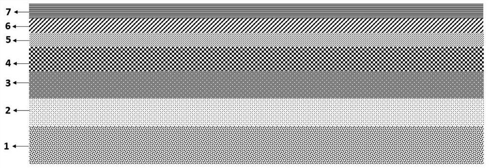
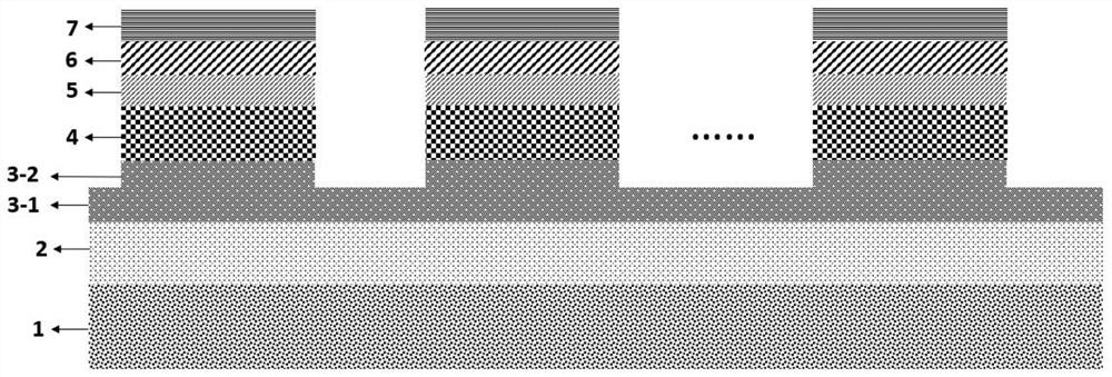
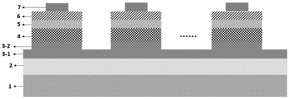
[0075]A Micro LED device that can suppress sidewall SRH non-radiative recombination.

[0076] The Micro LED device includes in sequence along the epitaxial growth direction: sapphire substrate 1; buffer layer 2, made of intrinsic GaN, with a thickness of 1.5 μm; N-type semiconductor material layer 3, made of n-GaN, with a total thickness of 5 μm , wherein the size of the sapphire substrate is a circle with a diameter of 2 inches, and the N-type semiconductor material layer 3 is divided into a first N-type semiconductor material layer 3-1 and a second N-type semiconductor material layer 3- 2. On the first N-type semiconductor material layer 3-1, there are evenly distributed matrix second N-type semiconductor material layers 3-2 with a side length of 20 microns; the first N-type semiconductor material layer and the second N-type semiconductor material layer -type semiconductor material layers have a thickness of 3 μm and 2 μm, respectively;

[0077] The second N-type semiconduc...

Embodiment 2

[0090] Except that the substrate is a gallium nitride substrate, the photolithography technology is a holographic photolithography technology, and the insulating confinement layer is hafnium oxide, the others are the same as in the first embodiment.

Embodiment 3

[0092] Except that the substrate is an R-plane aluminum oxide single crystal substrate and an insulating confinement layer of silicon nitride, the others are the same as in Embodiment 1.


PUM

PropertyMeasurementUnit
Thicknessaaaaaaaaaa
Thicknessaaaaaaaaaa
Thicknessaaaaaaaaaa

Abstract

The invention relates to a MicroLED device for inhibiting SRH non-radiative recombination and a preparation method. An epitaxial structure of the device sequentially comprises a substrate, a buffer layer, a first N-type semiconductor material layer and a second N-type semiconductor material layer along an epitaxial growth direction; the second N-type semiconductor material layer is sequentially covered with a multi-quantum well layer, a P-type current blocking layer and a P-type semiconductor material transmission layer; the center of each P-type semiconductor material transmission layer is covered with a P-type heavily doped semiconductor material transmission layer; a non-P-type heavily-doped semiconductor material transmission layer area on each P-type semiconductor material transmission layer is covered with an insulation limiting layer, and the upper surfaces of the insulation limiting layer and the semiconductor material transmission layer are current expansion layers. According to the invention, a better current limiting effect can be realized, SRH non-radiative recombination caused by side wall defects of the MicroLED device is reduced, and hole injection efficiency and external quantum efficiency (EQE) of the device are improved.

Description

technical field [0001] The technical solution of the present invention relates to a semiconductor device, specifically a micro semiconductor light emitting diode (Micro LED) and a preparation method thereof. Background technique [0002] Currently, there is an increasing demand for high-performance displays due to the rapid replacement of smartphones, tablet PCs, and increased demand for high-resolution display devices. Since the end of the last century, display technology has been continuously developing. Nowadays, the mainstream display screens are mainly divided into two types: one is liquid crystal display (LCD), which has the characteristics of long life, low cost, high portability and high brightness, but has poor conversion efficiency and poor color saturation and contrast. Low problem; the other is organic light-emitting diode (OLED) technology, OLED has the characteristics of self-illumination and high contrast, but there are still some defects in brightness and se...

Claims


Application Information

Patent Timeline
IPC IPC(8): H01L33/44H01L33/14H01L27/15H01L33/00
CPCH01L33/44H01L33/145H01L27/156H01L33/007H01L2933/0025
Inventor 张紫辉张沐垚李青张勇辉杭升郑权
Owner HEBEI UNIV OF TECH
Why Eureka
Try Eureka