
Heat treatment method and heat treatment apparatus

A heat treatment method and heat treatment device technology, applied in the direction of electric heating device, ohmic resistance heating device, measuring device, etc., can solve the problem that uniform device performance cannot be obtained

Pending Publication Date: 2021-10-29
DAINIPPON SCREEN MTG CO LTD
View PDF1 Cites 0 Cited by
  • Summary
  • Abstract
  • Description
  • Claims
  • Application Information

AI Technical Summary

Problems solved by technology

The surface attained temperature of the semiconductor wafer during flash heating directly contributes to the device performance, so if the surface attained temperature is uneven, there will be a problem that uniform device performance cannot be obtained

Method used


Image

  • Heat treatment method and heat treatment apparatus
  • Heat treatment method and heat treatment apparatus
  • Heat treatment method and heat treatment apparatus

Examples


no. 1 Embodiment approach >

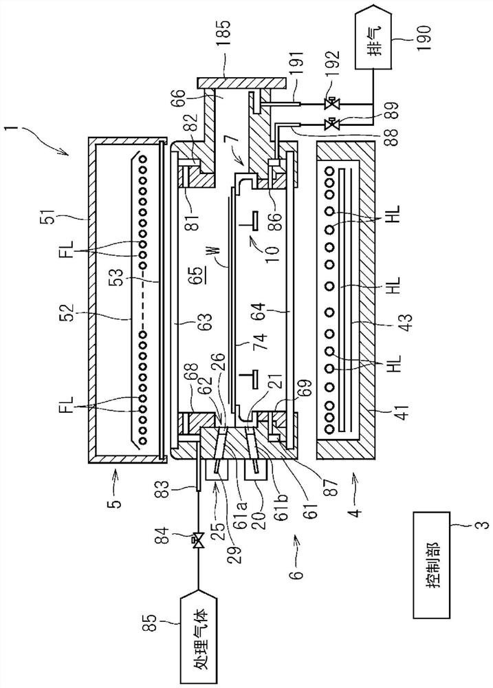
[0045]figure 1 It is a longitudinal sectional view showing the configuration of the heat treatment apparatus 1 of the present invention. figure 1 The heat treatment apparatus 1 is a flashlamp annealing apparatus that heats a semiconductor wafer W as a substrate by flash irradiation on a disk-shaped semiconductor wafer W. The size of the semiconductor wafer W to be processed is not particularly limited, and is, for example, φ300 mm or φ450 mm (φ300 mm in this embodiment). Impurities are implanted into the semiconductor wafer W before being loaded into the heat treatment apparatus 1 , and the implanted impurities are activated by heat treatment in the heat treatment apparatus 1 . also, figure 1 In each of the following drawings, the size or number of each part is exaggerated or simplified as necessary for easy understanding.

[0046] The heat processing apparatus 1 is provided with: the chamber 6 which accommodates the semiconductor wafer W, the flash heating part 5 which buil...

no. 2 Embodiment approach >

[0116] Next, a second embodiment of the present invention will be described. The configuration of the heat treatment apparatus of the second embodiment is completely the same as that of the first embodiment. In addition, the processing procedure of the semiconductor wafer W of the second embodiment is also substantially the same as that of the first embodiment. In the first embodiment, the current supply to the flash lamp FL is stopped when the actual measured value of the surface temperature of the semiconductor wafer W reaches the target temperature T2, but in the second embodiment, it is estimated that the surface temperature of the semiconductor wafer W reaches the target temperature T2. time, and the current supply to the flash lamp FL is stopped at the predetermined time.

[0117] Figure 14 It is a flowchart which shows the processing procedure of the heat processing apparatus 1 of 2nd Embodiment. Figure 14 Steps S21 to S23 with Figure 10 Steps S11 to S13 are the ...


PUM

PropertyMeasurementUnit
luminescence lifetimeaaaaaaaaaa

Abstract

According to the present invention, a semiconductor wafer is preliminarily heated at a preliminary heating temperature, and is then irradiated with flash light from a flash lamp. The surface temperature of the semiconductor wafer raised by the flash light irradiation is measured by means of an upper-radiating thermometer. When the surface temperature of the semiconductor wafer measured by means of the upper-radiating thermometer has reached a target temperature, electric current supply to the flash lamp is terminated and the surface temperature of the semiconductor wafer is allowed to decrease. Because electric current supply to the flash lamp is terminated when the actually measured temperature of the surface of the semiconductor wafer has reached the target temperature, it is possible to raise the surface temperature of the semiconductor wafer accurately to the target temperature, regardless of the surface state or reflectivity of the semiconductor wafer.

Description

technical field [0001] The present invention relates to a heat treatment method and heat treatment apparatus for heating a thin plate-shaped precision electronic substrate such as a semiconductor wafer (hereinafter, simply referred to as "substrate") by irradiating flash light. Background technique [0002] In the manufacturing process of semiconductor devices, impurity introduction is a necessary step for forming pn junctions in semiconductor wafers. Currently, impurity introduction is generally accomplished by ion implantation followed by annealing. The ion implantation method is a technique of ionizing impurity elements such as boron (B), arsenic (As), and phosphorus (P) and colliding with a semiconductor wafer at a high acceleration voltage to physically implant impurities. The implanted impurities are activated by annealing. At this time, if the annealing time is about several seconds or longer, the implanted impurities will be diffused deeply by heat, and as a result...

Claims


Application Information

Patent Timeline
Patent Type & Authority Applications(China)
IPC IPC(8): H01L21/26
CPCH01L21/67115H01L21/67248G05D23/27G05D23/1917H01L21/2686H01L22/12H01L21/324G01J5/0007H01L21/268H01L22/20H05B1/0233H05B3/0047H05B2203/032
Inventor 繁桝翔伍加藤慎一
Owner DAINIPPON SCREEN MTG CO LTD
Learn More