Cell structure of trench gate IGBT, preparation method thereof, and trench gate IGBT
A technology of trench gate and cell, which is applied in the direction of electrical components, semiconductor/solid-state device manufacturing, circuits, etc., and can solve the problem of increasing chip area
- Summary
- Abstract
- Description
- Claims
- Application Information
AI Technical Summary
Problems solved by technology
Method used
Image

Examples
Embodiment 1
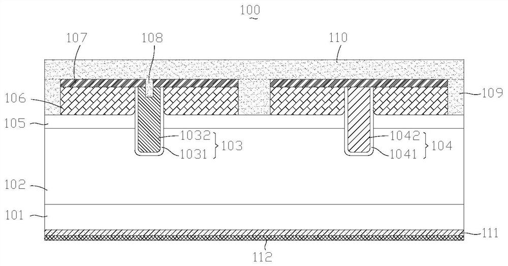
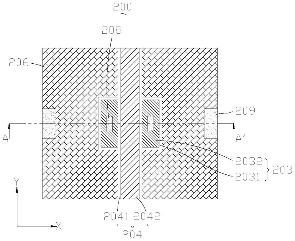
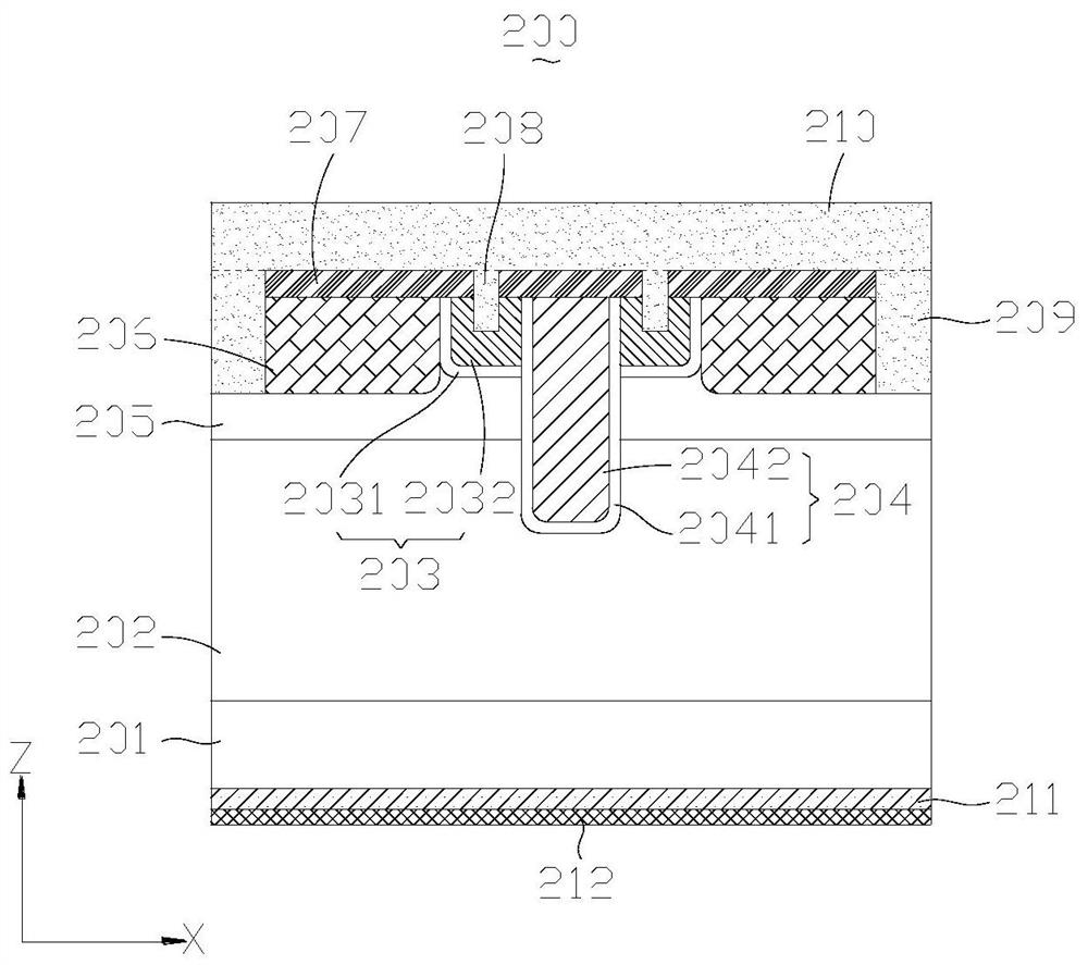
[0053] like figure 2 and image 3 As shown, an embodiment of the present disclosure provides a cell structure 200 of a trench gate IGBT, including a substrate 201 , a drift layer 202 , a first trench gate 203 , a second trench gate 204 , a well region 205 , and a source region 206 , a second source region 206 , an interlayer dielectric layer 207 , a first connection hole 208 , a second connection hole 209 , an emitter metal layer 210 , a collector region 211 and a collector metal layer 212 .
[0054] It should be noted that in order to figure 2 The shapes and positions of the first trench gate 203, the second trench gate 204, the source region 206, the first connection hole 208 and the second connection hole 209 are clearly displayed, so figure 2 The substrate 201 , the drift layer 202 , the interlayer dielectric layer 207 , the emitter metal layer 210 , the collector region 211 and the collector metal layer 212 are not shown. but combined image 3 The shapes and positi...
Embodiment 2
[0071] On the basis of Embodiment 1, this embodiment provides a method for fabricating a cell structure 200 of a trench gate IGBT. Figure 4 It is a schematic flowchart of a method for fabricating a cell structure 200 of a trench gate IGBT according to an embodiment of the present disclosure. Figure 5-Figure 15 It is a front plan view and a cross-sectional structural schematic diagram formed by the relevant steps of the preparation method of the cell structure 200 of the trench gate IGBT shown in the embodiment of the present disclosure. in, Image 6 , Figure 8 and Figure 10 It is a schematic top plan view of the front side formed by the relevant steps of the preparation method of the cell structure 200 of the trench gate IGBT. Below, refer to Figure 4 and Figure 5-Figure 15 The detailed steps of an exemplary method for fabricating the cell structure 200 of the trench gate IGBT according to the embodiment of the present disclosure will be described.
[0072] like ...
Embodiment 3
[0098] On the basis of the first embodiment, this embodiment provides a trench gate IGBT, which includes several cell structures 200 of the trench gate IGBT as described in the first embodiment.
[0099] Figure 16 The blocking voltage curves of a trench gate IGBT and a conventional trench gate IGBT are shown in an exemplary embodiment of the present disclosure, such as Figure 16 As shown, the two curves basically overlap, indicating that the trench gate IGBT provided by the present disclosure has the same blocking voltage capability as the conventional trench gate IGBT. Therefore, the first trench gate 203 and the second trench provided by the present disclosure have the same blocking voltage capability. The structure of the gate 204 integrated in one cell does not affect the blocking voltage capability of the trench gate IGBT.
[0100] Figure 17 is the saturation voltage curve diagram of a trench gate IGBT and a conventional trench gate IGBT shown in an exemplary embodim...
PUM
 Abstract
Description
Claims
Application Information
 - Generate Ideas
- Intellectual Property
- Life Sciences
- Materials
- Tech Scout
- Unparalleled Data Quality
- Higher Quality Content
- 60% Fewer Hallucinations
Browse by: Latest US Patents, China's latest patents, Technical Efficacy Thesaurus, Application Domain, Technology Topic, Popular Technical Reports.
© 2025 PatSnap. All rights reserved.Legal|Privacy policy|Modern Slavery Act Transparency Statement|Sitemap|About US| Contact US: help@patsnap.com