Crimping type power chip packaging structure
A technology of power chip and packaging structure, applied in electrical components, electric solid devices, circuits, etc., to achieve the effect of improving switching speed, reducing switching loss, and uniform force
- Summary
- Abstract
- Description
- Claims
- Application Information
AI Technical Summary
Problems solved by technology
Method used
Image
Examples
Embodiment Construction
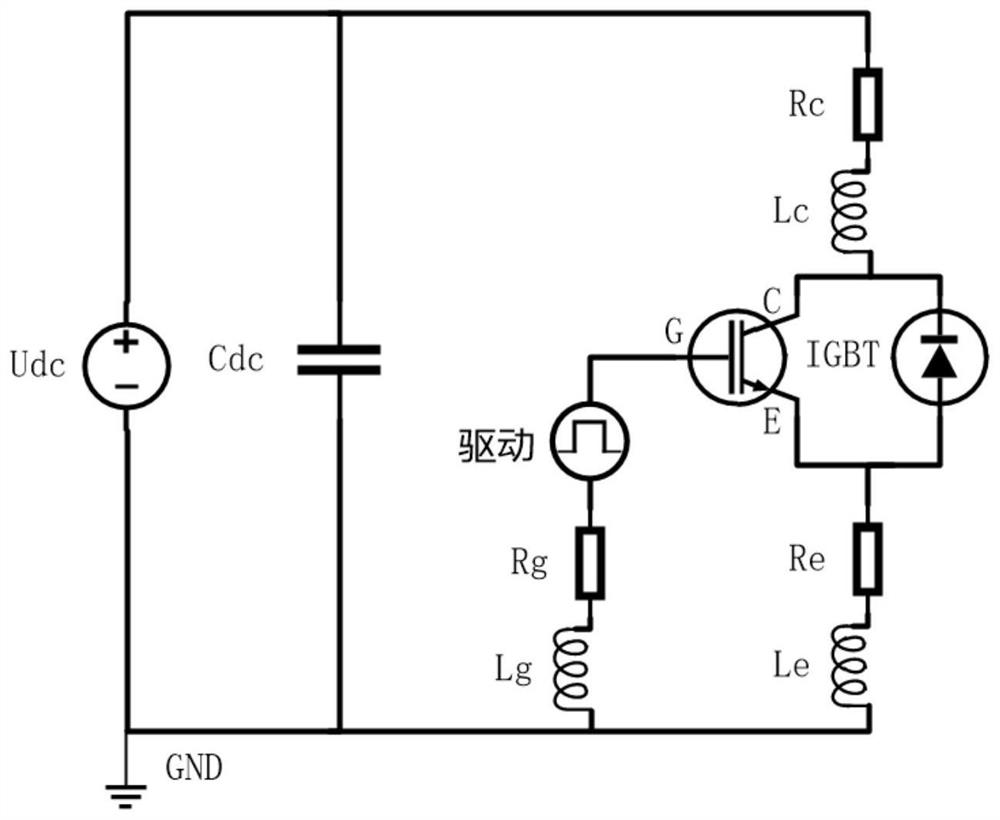
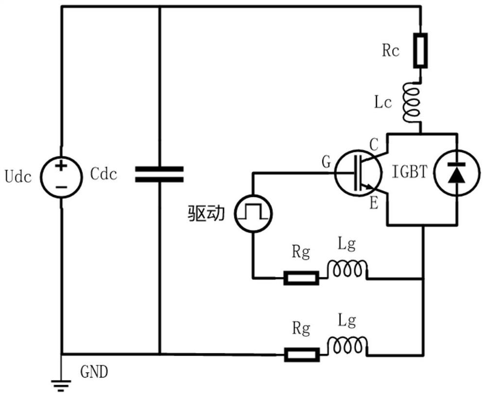
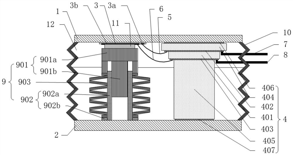
[0027] The inventors of the present application have found through research that as the current level increases, the IGBT device will generate a larger di / dt during the switching transient process. In the traditional packaging form, the emitter parasitic inductance is also included in the collector-emitter power loop and the gate drive loop, become the common emitter stray inductance, as figure 1 as shown, figure 1 "E" represents the emitter of the IGBT device, "C" represents the collector of the IGBT device, "G" represents the gate of the IGBT device, "Lg" represents the stray inductance of the drive circuit, and "Le" represents the stray common emitter Inductance, "Lc" stands for collector inductance. The di / dt with large switching transient will cause a large voltage drop on the common emitter stray inductance, which will have a great impact on the gate drive circuit, not only limiting the switching speed, And lead to more switching losses. In addition, oscillations in th...
PUM
 Abstract
Description
Claims
Application Information
 - R&D
- Intellectual Property
- Life Sciences
- Materials
- Tech Scout
- Unparalleled Data Quality
- Higher Quality Content
- 60% Fewer Hallucinations
Browse by: Latest US Patents, China's latest patents, Technical Efficacy Thesaurus, Application Domain, Technology Topic, Popular Technical Reports.
© 2025 PatSnap. All rights reserved.Legal|Privacy policy|Modern Slavery Act Transparency Statement|Sitemap|About US| Contact US: help@patsnap.com


