
Single-photon avalanche diode with back irradiation, and manufacturing method thereof

A single-photon avalanche and backside illumination technology, applied in the field of single-photon detection, can solve the problems of high dark count rate and low detection efficiency of single-photon avalanche diodes, and achieve the effects of suppressing tunneling effect, optimizing structure, and reducing electric field

Pending Publication Date: 2021-08-20
CHINA JILIANG UNIV
View PDF0 Cites 0 Cited by
  • Summary
  • Abstract
  • Description
  • Claims
  • Application Information

AI Technical Summary

Problems solved by technology

[0003] The traditional single photon avalanche diode has a high dark count rate, and the current research is more on the single photon avalanche diode illuminated by the front of the light. When the single photon avalanche diode of this structure is integrated with the quenching circuit and the readout circuit, the circuit is manufactured Around the single photon avalanche diode, the photosensitive area of ​​the single photon avalanche diode only occupies a small part of the entire pixel, making its detection efficiency very low

Method used


Image

  • Single-photon avalanche diode with back irradiation, and manufacturing method thereof
  • Single-photon avalanche diode with back irradiation, and manufacturing method thereof
  • Single-photon avalanche diode with back irradiation, and manufacturing method thereof

Examples


Embodiment Construction

[0035] In order to better understand the content of the patent of the present invention, the technical solution of the present invention will be further described below in conjunction with the accompanying drawings.

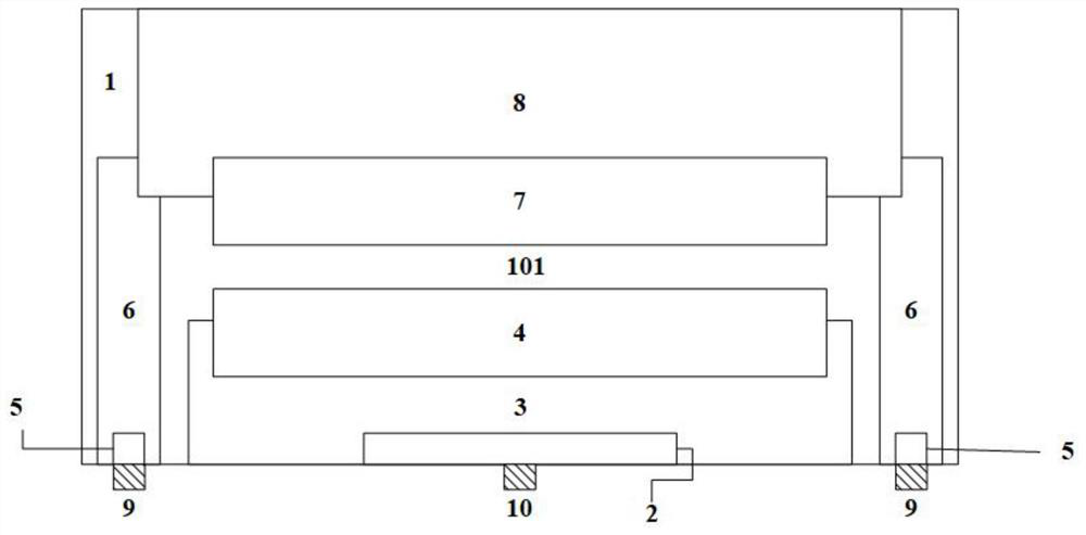
[0036] Such as figure 1 As shown, the back-illuminated single photon avalanche diode includes a P-type epitaxial layer 1, a P+ heavily doped region 2 is arranged inside the P-type epitaxial layer 1, and a P-lowly doped region is coaxially arranged on the periphery of the P+ heavily doped region 2 3. A P-type avalanche doped region 4 is arranged coaxially below the P-lowly doped region 3, an N+ heavily doped region 5 is arranged on both sides of the P+ heavily doped region 2, and a coaxially arranged below the N+ heavily doped region 5 N well region 6, N-type avalanche doped region 7 is arranged at intervals below the P-type avalanche doped region 4, and N− low doped region 8 is arranged below the N-type avalanche doped region 7.

[0037] The P+ heavily doped reg...


PUM


Abstract

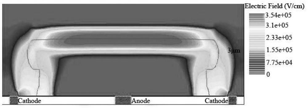
The invention discloses a single-photon avalanche diode with back irradiation, and a manufacturing method thereof, and belongs to the technical field of single-photon detection. The single-photon avalanche diode comprises a P-type epitaxial layer, a P+ heavily doped region is arranged in the P-type epitaxial layer, a P- lightly doped region is coaxially arranged on the periphery of the P+ heavily doped region, a P-type avalanche doped region is coaxially arranged below the P- lightly doped region, N+ heavily doped regions are arranged on the two sides of the P+ heavily doped region, an N well region is coaxially arranged below the N+ heavily doped regions, N-type avalanche doped regions are arranged below the P-type avalanche doped region at intervals, and an N- lightly doped region is arranged below the N-type avalanche doped regions. The mode that light irradiates from the back face is adopted, the device structure is optimized, and a peripheral circuit of the device is integrated below the device. And the detection efficiency of the device is improved. The P-type avalanche doped region, the P-type epitaxial layer central region and the N-type avalanche doped regions form an avalanche junction, and the dark counting rate of the device is remarkably reduced by adopting the sub-structure.

Description

technical field [0001] The invention belongs to the technical field of single photon detection, and in particular relates to a low dark count rate single photon avalanche diode illuminated on the back and a manufacturing method thereof. Background technique [0002] Single-photon detection technology has broad application prospects in national defense construction, industry and civilian life, such as quantum key distribution, laser radar, fluorescence lifetime imaging and three-dimensional vision systems. As a core device for single photon detection, single photon avalanche diode (single photon avalanche photodiode, denoted as SPAD) based on CMOS technology has attracted more and more attention and attention of researchers. The single photon avalanche diode in Geiger mode is a detector that can detect extremely weak light signals. It has large internal gain, high sensitivity, fast response speed, high detection efficiency, low noise, small size, strong structure and easy int...

Claims


Application Information

Patent Timeline
IPC IPC(8): H01L31/107H01L31/0352H01L31/18H01L27/146
CPCH01L27/1464H01L31/03529H01L31/107H01L31/1804Y02P70/50
Inventor 赵天琦储童冯桂兰潘劲旅林春兰郭锴悦
Owner CHINA JILIANG UNIV
Learn More