Semiconductor structure and forming method thereof
A semiconductor and graphic layer technology, applied in semiconductor/solid-state device manufacturing, electrical components, circuits, etc., to solve problems such as increasing the difficulty and complexity of integrated circuits
- Summary
- Abstract
- Description
- Claims
- Application Information
AI Technical Summary
Problems solved by technology
Method used
Image

Examples
Embodiment Construction
[0033] It can be seen from the background art that how to improve the matching degree between the pattern formed on the wafer and the target pattern becomes a challenge. Specifically, the pattern transfer accuracy of the current patterning process is low. Combining with a method of forming a semiconductor structure, the reasons for the low accuracy of pattern transfer are analyzed.
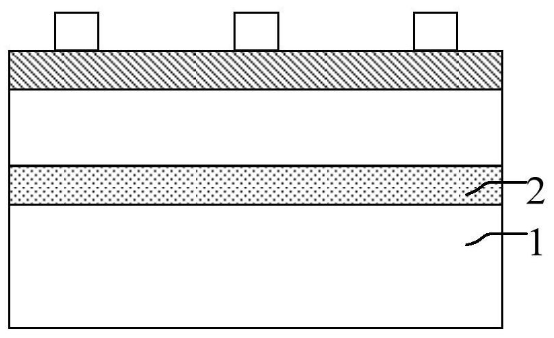
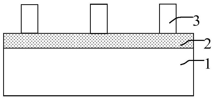
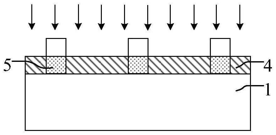
[0034] refer to Figure 1 to Figure 7 , shows a structural schematic diagram corresponding to each step in a method for forming a semiconductor structure.
[0035] refer to figure 1 , providing a substrate 1 ; forming a hard mask material layer 2 on the substrate 1 .
[0036] combined reference Figure 1 to Figure 2 , forming a flat layer 3 on the hard mask material layer 3 .
[0037] refer to image 3 , using the flat layer 3 as a mask to perform ion implantation on the hard mask material layer 2, which is suitable for increasing the etching resistance of the hard mask material layer 2, and...
PUM
 Abstract
Description
Claims
Application Information
 - Generate Ideas
- Intellectual Property
- Life Sciences
- Materials
- Tech Scout
- Unparalleled Data Quality
- Higher Quality Content
- 60% Fewer Hallucinations
Browse by: Latest US Patents, China's latest patents, Technical Efficacy Thesaurus, Application Domain, Technology Topic, Popular Technical Reports.
© 2025 PatSnap. All rights reserved.Legal|Privacy policy|Modern Slavery Act Transparency Statement|Sitemap|About US| Contact US: help@patsnap.com