Silicon-doped magnetron sputtering process for improving reliability of TaOx-based resistive random access memory

A technology of resistive variable memory and magnetron sputtering, which is applied in sputtering plating, metal material coating process, ion implantation plating, etc., which can solve the constraints of less read and write times, high operating voltage, operating voltage and durability The commercial application of devices and other issues, to achieve the effect of improving reliability, reducing operating voltage, and fast film deposition speed

Active Publication Date: 2021-07-09
DALIAN UNIV OF TECH
View PDF6 Cites 2 Cited by
  • Summary
  • Abstract
  • Description
  • Claims
  • Application Information

AI Technical Summary

Problems solved by technology

[0004] Although RRAM devices have been extensively studied, the high operating voltage and endurance of the devices have been restricting the commercial application of the devices.
Someone improved TaO by metal doping x The switching uniformity of the base RRAM, but there is a problem of low read and write times
Compared with other metal doping methods, Kim, B.Y. and K.J.Lee et al mentioned in the article that silicon-doped TaO was prepared by atomic layer deposition. x Base RRAM can reduce the operating current, but the operating voltage is relatively large (Journal: JapaneseJournal of Applied Physics, 2016, 55(4s))

Method used


Image

  • Silicon-doped magnetron sputtering process for improving reliability of TaOx-based resistive random access memory
  • Silicon-doped magnetron sputtering process for improving reliability of TaOx-based resistive random access memory
  • Silicon-doped magnetron sputtering process for improving reliability of TaOx-based resistive random access memory

Examples


Embodiment 1

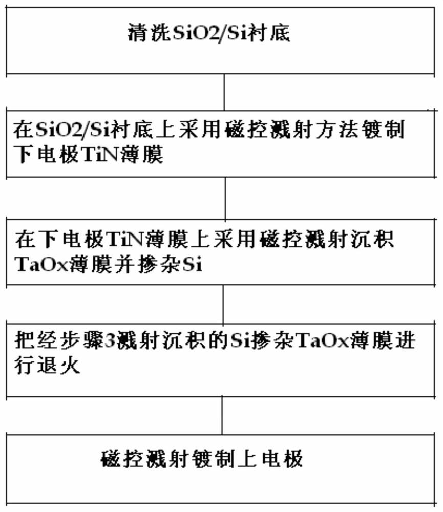
[0038] Such as figure 1 As shown, an improved TaO x The silicon-doped magnetron sputtering process for the reliability of the base resistive variable memory comprises the following steps:

[0039] Step 1. Clean SiO2 2 / Si substrate, specifically comprising the following sub-steps:

[0040] (a) SiO 2 Put the Si substrate in deionized water and ultrasonically clean it for 5 minutes;

[0041] (b) SiO cleaned by substep (a) 2 Put the Si substrate in acetone and ultrasonically clean it for 5 minutes;

[0042] (c) SiO cleaned by substep (b) 2 Put the Si substrate in absolute ethanol and ultrasonically clean it for 5 minutes;

[0043] (d) SiO cleaned by substep (c) 2 / Si substrate is rinsed with deionized water, and then dried with N2 gas;

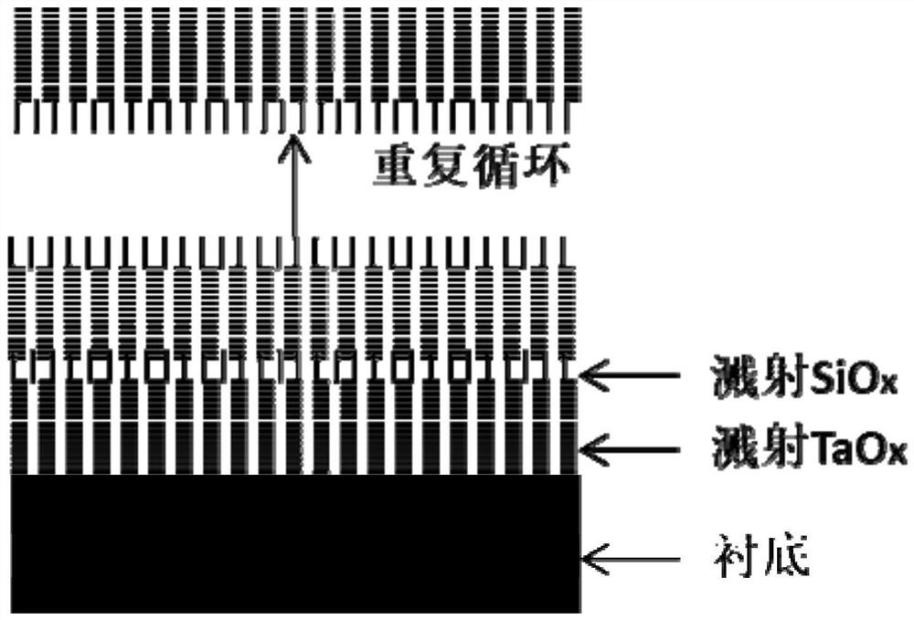
[0044] Step 2, on SiO 2 On the Si substrate, the TiN film of the lower electrode is plated by the magnetron sputtering method, which specifically includes the following sub-steps:

[0045] (a) SiO cleaned in step 1 2 / Si substrate is p...

Embodiment 2

[0060] Step 1 to step 4 in this embodiment are identical to step 1 to step 4 in embodiment 1;

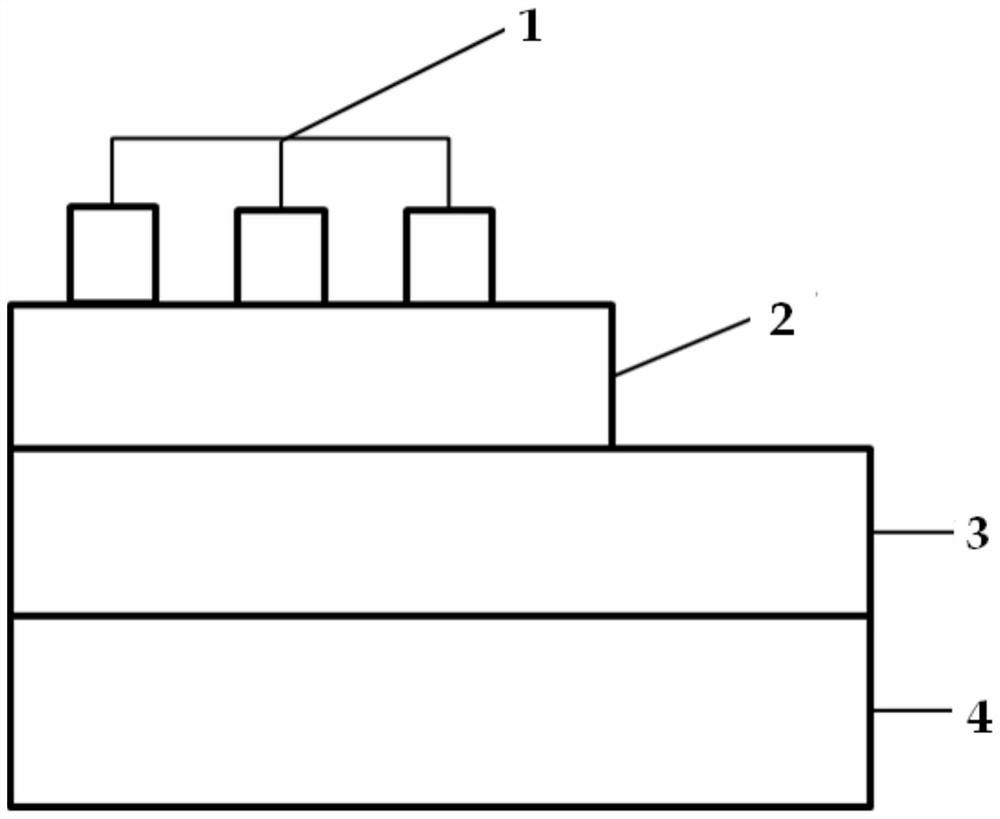
[0061] Step 5, plating the Pt upper electrode by magnetron sputtering, specifically includes the following sub-steps:

[0062] (a) Si-doped TaO annealed in step 4 x The film is placed in a magnetron sputtering vacuum chamber;

[0063] (b) Evacuate the vacuum chamber to 5×10 -4 Pa, the substrate temperature is room temperature, argon gas is introduced into the vacuum chamber, the flow rate is 10sccm, the power is adjusted to 18W, the pre-sputtering is 10min and the formal sputtering is 40min, the thickness of the deposited Pt upper electrode is 150nm, and the current-voltage test curve Such as Figure 5 shown.

Embodiment 3

[0065] Step 1 to step 4 in this embodiment are identical to step 1 to step 4 in embodiment 1;

[0066] Step 5, plating the Al upper electrode by magnetron sputtering, specifically includes the following sub-steps:

[0067] (a) Si-doped TaO annealed in step 4 x The film is placed in a magnetron sputtering vacuum chamber;

[0068] (b) Evacuate the vacuum chamber to 5×10 -4 Pa, the substrate temperature is room temperature, argon gas is introduced into the vacuum chamber, the flow rate is 12sccm, the power is adjusted to 18W, the pre-sputtering is 10min and the formal sputtering is 42min, the thickness of the upper electrode deposited on Al is 150nm, and the current-voltage test curve Such as Figure 6 shown.


PUM

PropertyMeasurementUnit
thicknessaaaaaaaaaa
thicknessaaaaaaaaaa
thicknessaaaaaaaaaa

Abstract

The invention belongs to the technical field of microelectronic and semiconductor processing, and relates to a silicon-doped magnetron sputtering process for improving the reliability of a TaOx-based resistive random access memory. The process comprises the following steps: (1) cleaning a SiO2 / Si substrate, (2) plating a lower electrode TiN film on the SiO2 / Si substrate by adopting a magnetron sputtering method, (3) depositing a TaOx film on the lower electrode TiN film by adopting magnetron sputtering and doping Si, (4) annealing the Si-doped TaOx film subjected to sputtering deposition in the step (3), and (5) plating an upper electrode by magnetron sputtering. According to the method, Si is doped in the TaOx thin film, the defect structure in the TaOx thin film can be effectively adjusted, the oxygen vacancy concentration is increased, the operating voltage of the device is reduced, the memory window is enlarged, the reliability of the device is improved, the technological process is simple, the thin film deposition speed is high, and technical support can be provided for large-scale application and popularization of the resistive random access memory.

Description

technical field [0001] The present invention relates to a kind of improved TaO x The invention discloses a reliable silicon-doped magnetron sputtering process for a base resistive variable memory, belonging to the technical field of microelectronics and semiconductor processing. [0002] technical background [0003] Since entering the information age, people's requirements for storage and computing have increased rapidly, and traditional forms of memory are limited by the small size effect and cannot meet people's needs. Resistive RAM (RRAM) is one of the most promising candidates for next-generation nonvolatile memory due to its fast write / erase speed and simple structure. Ta 2 o 5 It is a widely used resistive material, and there are many preparation methods, such as thermal oxidation, chemical vapor deposition, magnetron sputtering, electron beam evaporation and atomic layer deposition. Among them, magnetron sputtering is widely applied to TaO because of its simple pr...

Claims


Application Information

Patent Timeline
Patent Type & Authority Applications(China)
IPC IPC(8): C23C14/35C23C14/02C23C14/06C23C14/08C23C14/16C23C14/18C23C14/58
CPCC23C14/0036C23C14/021C23C14/0641C23C14/083C23C14/165C23C14/185C23C14/35C23C14/352C23C14/5806
Inventor 王德君谢威威周大雨白娇蔡承轩李苏洋
Owner DALIAN UNIV OF TECH
Why Eureka
Try Eureka