
Silicon-based thin-film solar cell with double-layer split grating structure

A technology of solar cells and silicon-based thin films, applied in photovoltaic power generation, circuits, electrical components, etc., can solve the problems of low light absorption efficiency, and achieve obvious effects of enhanced absorption, improved light absorption efficiency, and obvious effects

Active Publication Date: 2021-06-04
HEFEI UNIV OF TECH
View PDF6 Cites 0 Cited by
  • Summary
  • Abstract
  • Description
  • Claims
  • Application Information

AI Technical Summary

Problems solved by technology

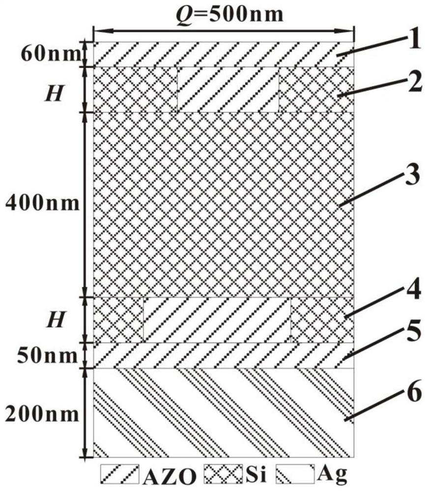
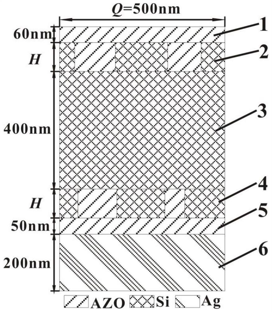
[0007] In order to solve the problem of low light absorption efficiency of silicon-based thin-film solar cells in the near-infrared band in the prior art, the present invention proposes a silicon-based thin-film solar cell with a double-layer split grating structure

Method used


Image

  • Silicon-based thin-film solar cell with double-layer split grating structure
  • Silicon-based thin-film solar cell with double-layer split grating structure
  • Silicon-based thin-film solar cell with double-layer split grating structure

Examples


Embodiment Construction

[0027] The following will clearly and completely describe the technical solutions in the embodiments of the present invention with reference to the accompanying drawings in the embodiments of the present invention. Obviously, the described embodiments are only some, not all, embodiments of the present invention.

[0028]In describing the present invention, it should be understood that the terms "upper", "lower", "front", "rear", "left", "right", "top", "bottom", "inner", " The orientation or positional relationship indicated by "outside", etc. is based on the orientation or positional relationship shown in the drawings, and is only for the convenience of describing the present invention and simplifying the description, rather than indicating or implying that the referred device or element must have a specific orientation, so as to Specific orientation configurations and operations, therefore, are not to be construed as limitations on the invention.

[0029] The silicon-based t...


PUM

PropertyMeasurementUnit
thicknessaaaaaaaaaa
thicknessaaaaaaaaaa
thicknessaaaaaaaaaa

Abstract

The invention discloses a silicon-based thin film solar cell with a double-layer split grating structure. The silicon-based thin film solar cell comprises an Ag substrate layer, and an AZO passivation layer, a lower grating layer, a silicon absorption layer, an upper grating layer and an AZO anti-reflection layer are arranged on the Ag substrate layer in a layer-by-layer mode. The lower grating layer and the upper grating layer respectively comprise at least one grating period, and each grating period is formed by sequentially and alternately arranging Si strips and AZO strips along the width direction of the silicon-based thin film solar cell. In the structure of the silicon-based thin-film solar cell, phase mismatching and width unequal between the upper grating layer and the lower grating layer can form more diffraction orders, so that the light absorption efficiency of the silicon-based thin-film solar cell in a full wave band is improved, and particularly, the absorption efficiency of the silicon-based thin-film solar cell in a near-infrared wave band is obviously improved.

Description

technical field [0001] The invention relates to the technical field of silicon-based thin-film solar cells, in particular to a silicon-based thin-film solar cell with a double-layer split grating structure. Background technique [0002] In recent years, due to problems such as energy depletion and environmental pollution, human beings are urgently looking for and developing renewable clean energy for industrial production and residents' lives. Solar cells convert solar energy into electrical energy and obtain clean energy, which has attracted widespread attention at home and abroad. The design principle of solar cells is to improve photoelectric conversion efficiency while reducing processing and manufacturing costs. Common solar cells include silicon-based solar cells, dye-sensitized solar cells, gallium arsenide solar cells, cadmium telluride solar cells, and perovskite solar cells. [0003] Due to the advantages of low cost, abundant reserves, non-toxicity and mature pr...

Claims


Application Information

Patent Timeline
Patent Type & Authority Applications(China)
IPC IPC(8): H01L31/0224H01L31/0232H01L31/0445
CPCH01L31/02327H01L31/022466H01L31/0445Y02E10/50
Inventor 郑红梅于迎春陈科吴胜郑念红田文立刘志杰
Owner HEFEI UNIV OF TECH
Learn More