Printed circuit board substrate comprising a coated boron nitride
A printed circuit, board substrate technology, applied in the field of printed circuit board substrates containing coated boron nitride, can solve the problems of reduced mechanical properties, reduced peel strength, etc.
- Summary
- Abstract
- Description
- Claims
- Application Information
AI Technical Summary
Problems solved by technology
Method used
Image
Examples
Embodiment 1 to 6
[0065] Examples 1 to 6: Effect of coating thickness on coated hexagonal boron nitride
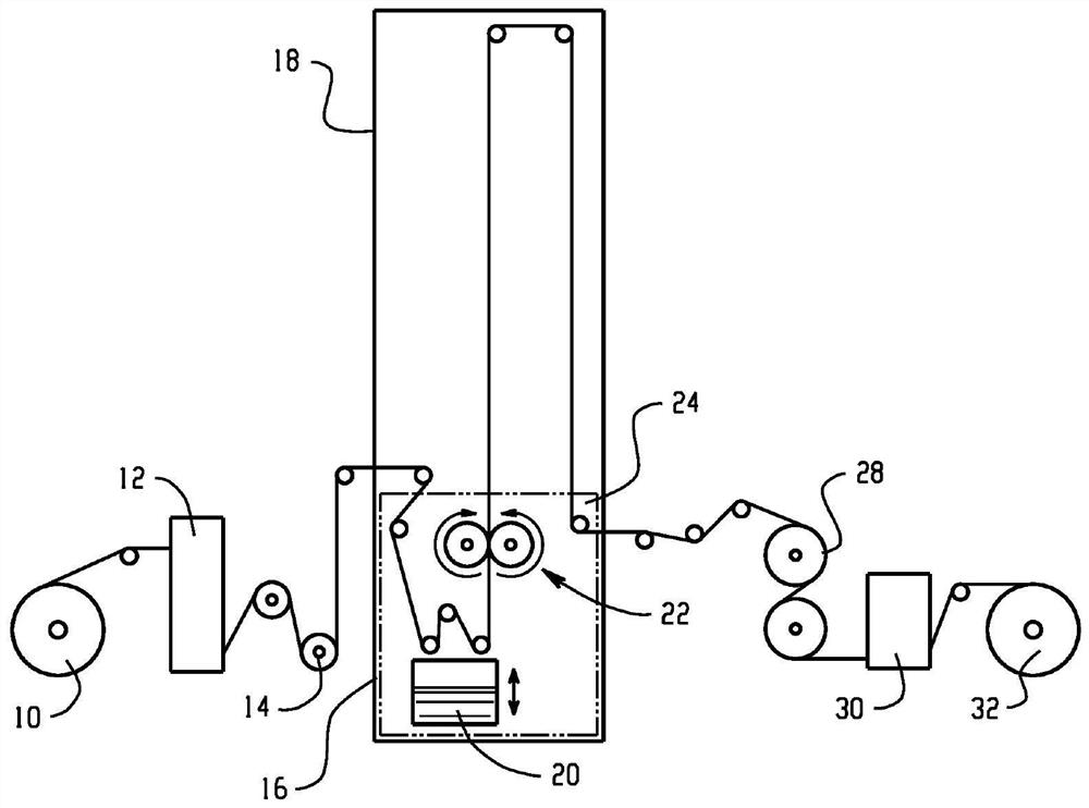
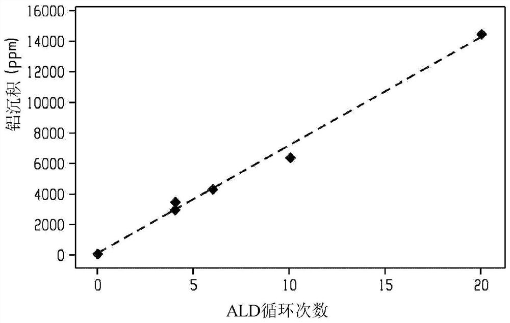
[0066]The surface of hexagonal boron nitride particles was coated with aluminum oxide by atomic layer deposition (ALD) using trimethylaluminum and water as precursors. The boron nitride powder used was PBN20, which is a high density agglomerate of hexagonal boron nitride flakes supplied by Zibo Jonye Ceramics Technology Company. PBN20 exhibits a typical median particle size of 18 microns to 22 microns, and 6.2 square meters per gram (m 2 / g) specific surface area. By gradually varying the number of ALD cycles, a series of coated powders with different coating thicknesses were produced. The aluminum content of the coated powders was determined by ICP analysis and the surface energy was measured by the Washburn wicking method for the contact angles of the different probe liquids. The contact angle measurements were combined with Fowkes theory to decompose the surface energy into dispersive...
Embodiment 7
[0070] Example 7: Printed Circuit Board Substrates Comprising Coated Boron Nitride
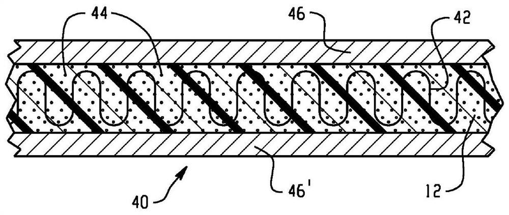
[0071] A printed circuit board substrate was prepared comprising 15 volume percent coated boron nitride and 85 volume percent RO4000 (commercially available from Rogers Corporation), both based on the total volume of the substrate minus the glass fiber reinforcement. Coated boron nitride was prepared by coating boron nitride powder (Momentive PT-120) with 10 ALD cycles of alumina. The aluminum oxide coating has a thickness of 5 nm. Thermal conductivity and peel strength are shown in Table 2.
Embodiment 8
[0072] Example 8: Printed Circuit Board Substrate Comprising Uncoated Boron Nitride
[0073] A printed circuit board substrate was prepared comprising 15 volume percent uncoated boron nitride and 85 volume percent RO4000 (commercially available from Rogers Corporation). The uncoated boron nitride is Momentive PT-100. Thermal conductivity and peel strength are shown in Table 2.
[0074]
[0075] Table 2 shows that the peel strength of the printed circuit board substrate of Example 7 comprising the coated boron nitride compared to the printed circuit board substrate of Example 8 comprising the same amount of boron nitride but not coated was improved. language has been significantly improved.
PUM
| Property | Measurement | Unit |
|---|---|---|
| particle size | aaaaa | aaaaa |
| thickness | aaaaa | aaaaa |
| thickness | aaaaa | aaaaa |
Abstract
Description
Claims
Application Information
 - R&D
- Intellectual Property
- Life Sciences
- Materials
- Tech Scout
- Unparalleled Data Quality
- Higher Quality Content
- 60% Fewer Hallucinations
Browse by: Latest US Patents, China's latest patents, Technical Efficacy Thesaurus, Application Domain, Technology Topic, Popular Technical Reports.
© 2025 PatSnap. All rights reserved.Legal|Privacy policy|Modern Slavery Act Transparency Statement|Sitemap|About US| Contact US: help@patsnap.com


