Microfluid adapter plate integrated with high-power radio frequency chip and preparation method of microfluid adapter plate

A radio frequency chip, microfluidic technology, applied in the field of microelectronics and microsystems

Active Publication Date: 2021-05-07
NO 55 INST CHINA ELECTRONIC SCI & TECHNOLOGYGROUP CO LTD
View PDF10 Cites 3 Cited by
  • Summary
  • Abstract
  • Description
  • Claims
  • Application Information

AI Technical Summary

Problems solved by technology

Therefore, the complete set of technology for the integration of high-power RF power chips is a bottleneck restricting the development of current high-power RF systems.

Method used


Image

  • Microfluid adapter plate integrated with high-power radio frequency chip and preparation method of microfluid adapter plate
  • Microfluid adapter plate integrated with high-power radio frequency chip and preparation method of microfluid adapter plate
  • Microfluid adapter plate integrated with high-power radio frequency chip and preparation method of microfluid adapter plate

Examples


Embodiment Construction

[0038] The specific content of the present invention will be further described below in conjunction with the accompanying drawings and specific embodiments.

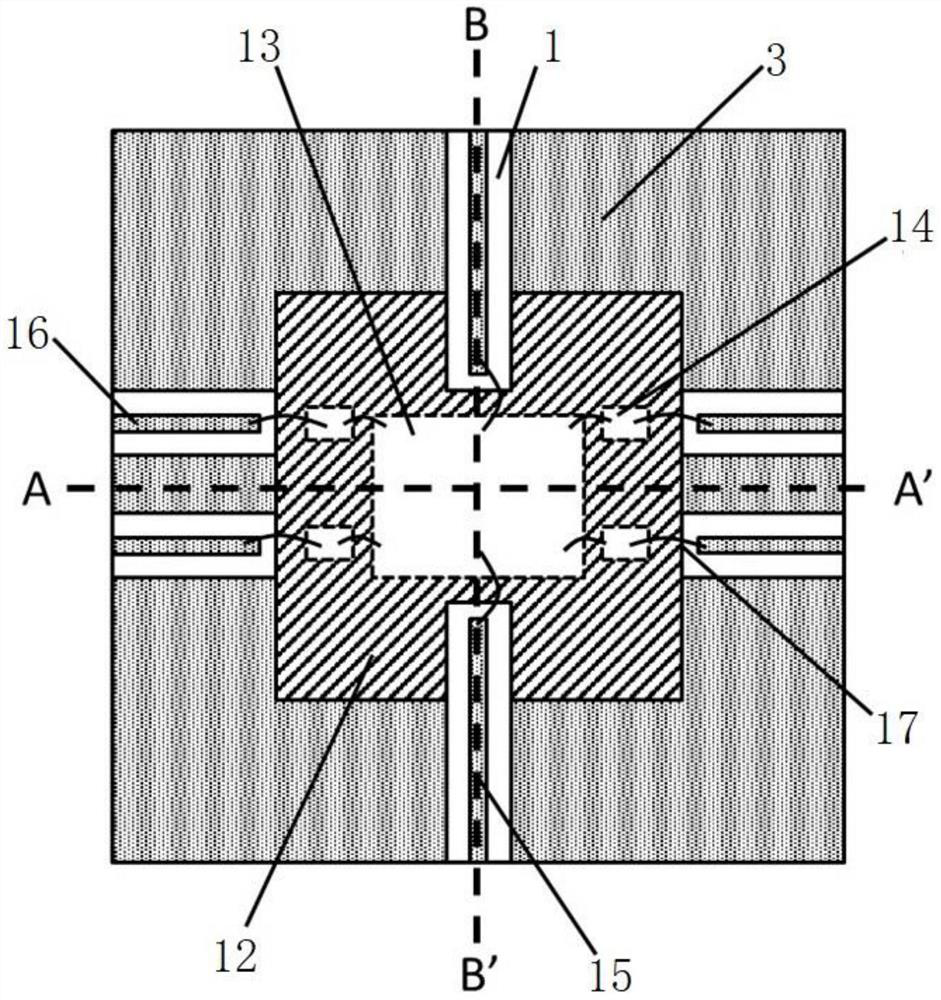
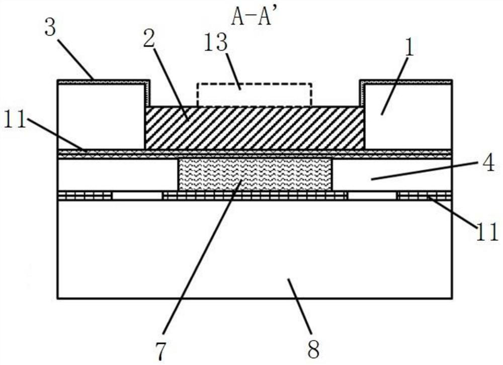
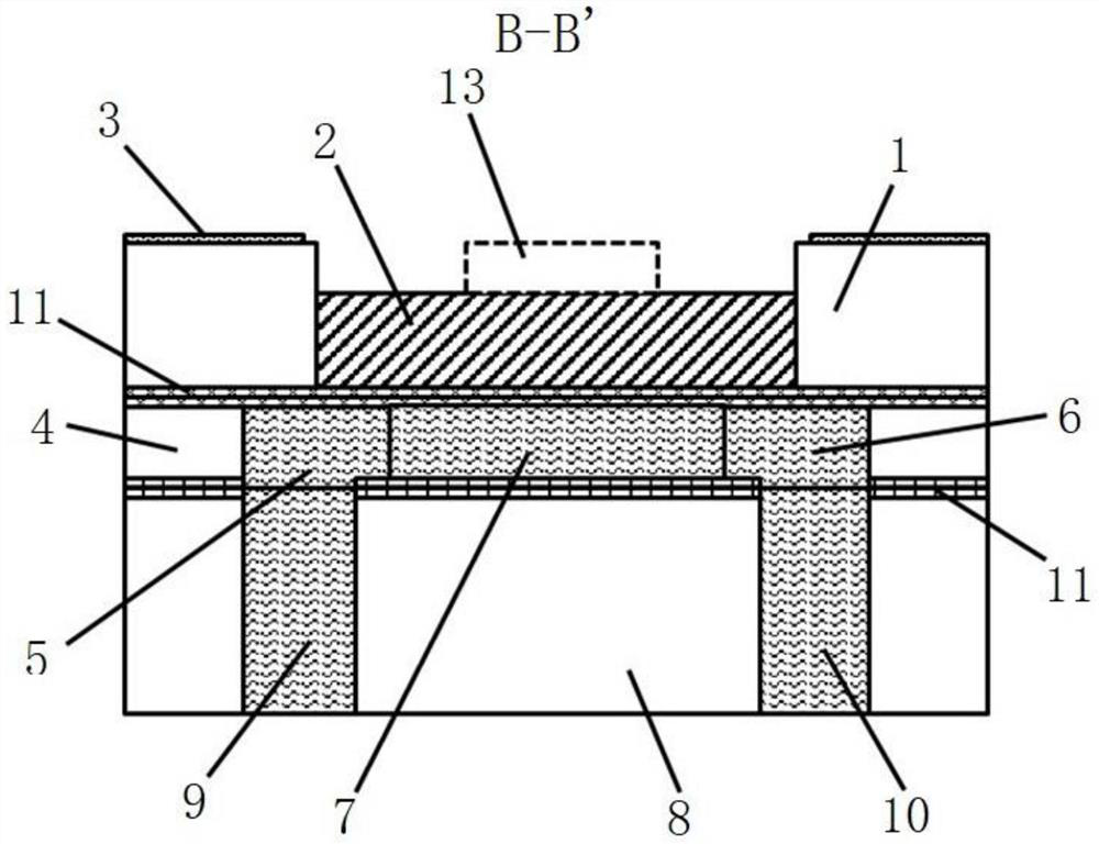
[0039] On the one hand, embodiments of the present invention provide a microfluidic adapter board integrating high-power radio frequency chips, such as Figure 1-4 As shown, including the signal interconnection layer, the microfluidic channel structure layer and the microfluidic interface structure layer arranged from top to bottom;

[0040] The signal interconnection layer includes a top-layer silicon chip 1 covered with a ground metal layer 3 and a thick copper structure 2 embedded in the top-layer silicon chip 1. The upper surface of the thick copper structure 2 is provided with a chip bonding surface 12 and is connected to The ground metal layer 3 is connected;

[0041] The micro-flow channel structure layer includes an intermediate layer silicon chip 4 and a shunt flow channel 5 and a confluence flow channel 6 arra...


PUM

PropertyMeasurementUnit
Thicknessaaaaaaaaaa
Thicknessaaaaaaaaaa
Thicknessaaaaaaaaaa

Abstract

The invention provides a microfluid adapter plate integrated with a high-power radio frequency chip and a preparation method of the microfluid adapter plate. The microfluid adapter plate comprises a signal interconnection layer, a micro-channel structure layer and a microfluid interface structure layer, wherein the signal interconnection layer comprises a top silicon wafer and a thick copper structural member, the surface of the top silicon wafer is covered with a grounding metal layer, the thick copper structural member is embedded into the top silicon wafer, and the upper surface of the thick copper structural member is provided with a chip bonding surface and is connected with the grounding metal layer; the micro-channel structure layer comprises a middle-layer silicon wafer as well as a shunting channel and a converging channel which are arranged in the middle-layer silicon wafer, a plurality of cooling channels are arranged between the shunting channel and the converging channel in parallel, and the shunting channel, the cooling channels and the converging channel are communicated in sequence; and the microfluid interface structure layer comprises a bottom layer silicon wafer, a liquid inlet corresponding to the shunting flow channel and a liquid outlet corresponding to the converging flow channel. According to the invention, the thick copper structure and the micro-channel are combined, waste heat of a heating device can be taken away in time through the cooling liquid working medium with high heat capacity, and the heat dissipation efficiency can be remarkably improved.

Description

technical field [0001] The invention relates to the technical field of microelectronics and microsystems. Background technique [0002] With the development of technology, systems in the fields of radar, electronic countermeasures and communications gradually present high density, multi-function, high reliability and low cost. As the core component of the RF system, RF power chips are mostly GaN high electron mobility transistor (HEMT) multi-stage amplifiers. Among them, the heating power of the GaN HEMT transistor gate can reach 60-80 W. As the RF power device increases by 1°C on the basis of the safe operating temperature, its RF output characteristics will decrease exponentially, and its reliability will decrease by about 5%. If the heat generated by the electronic device cannot be dissipated in time, it will Directly affect the performance of the radio frequency system, and even cause damage. In the GaN RF power chip, the source of the GaN HEMT transistor is grounded ...

Claims


Application Information

Patent Timeline
IPC IPC(8): H01L23/498H01L23/367H01L23/373H01L23/473H01L23/58H01L21/48B81B7/02B81C1/00
CPCH01L23/49822H01L23/49844H01L23/49866H01L23/367H01L23/3736H01L23/473H01L23/585H01L21/4857B81B7/02B81C1/00119B81B2201/05
Inventor 禹淼石归雄张洪泽黄旼朱健
Owner NO 55 INST CHINA ELECTRONIC SCI & TECHNOLOGYGROUP CO LTD
Why Eureka
Try Eureka