a tio 2 /ps colloidal photonic crystal and its preparation method and application in humidity sensor
A colloidal photonic crystal, humidity sensor technology, applied in crystal growth, chemical instruments and methods, color/spectral property measurement, etc., to achieve the effects of improving optical properties, good sensing performance, and increasing effective refractive index
- Summary
- Abstract
- Description
- Claims
- Application Information
AI Technical Summary
Problems solved by technology
Method used
Image
Examples
Embodiment 1
[0032] Example 1 TiO 2 Preparation of / PS Colloidal Photonic Crystals
[0033] Step 1: Microfluidic injection to prepare PS colloidal crystal monolayers
[0034] The 690nm PS microspheres, absolute ethanol, and n-butanol were subjected to ultrasonic oscillation in a volume ratio of 2:1:1 to form a PS microsphere suspension. The liquid surface forms a single-layer PS microsphere film.
[0035] The single-layer PS microsphere film exhibits different colors at different angles due to its unique periodic arrangement under the illumination of white light.
[0036] Step 2: Reactive Ion Etching
[0037] By lifting the substrate, the single-layer PS microsphere film is transferred to the target substrate (silicon wafer) as a reactive ion etching mask, and the O 2 For the reaction gas, the etching radio frequency power is 15W, the oxygen flow rate is 30sccm, the reaction chamber pressure is 2Pa, and the etching time is 0min.
[0038] like figure 2 As shown, the single-layer PS m...
Embodiment 2
[0041] Example 2 TiO 2 Preparation of / PS Colloidal Photonic Crystals
[0042] The difference from Example 1 is that the etching time in Step 2 is 1 min.
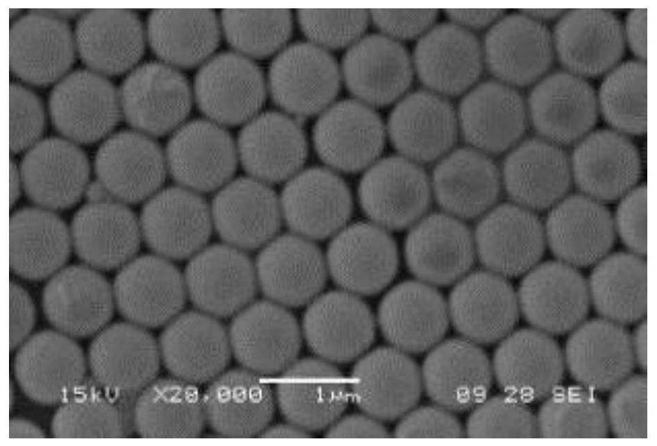
[0043] like image 3As shown, the single-layer PS microsphere film on the PS mask is a periodic hexagonal close-packed microsphere film, the diameter of the microspheres is 670 nm, the overall cracks and defects are few, and the assembly effect is good.
[0044] like Figure 4 As shown, the TiO prepared after etching for 1 min 2 / PS colloidal photonic crystal, the microsphere gap is enlarged, and the surface and gap of the microsphere are covered with TiO 2 film.
Embodiment 3
[0045] Example 3 TiO 2 Preparation of / PS Colloidal Photonic Crystals
[0046] The difference from Example 1 is that the etching time in Step 2 is 2 min.
[0047] like Figure 5 As shown, the single-layer PS microsphere film on the PS mask plate is a periodic hexagonal close-packed microsphere film, the diameter of the microspheres is 640 nm, the overall cracks and defects are few, and the assembly effect is good.
PUM
| Property | Measurement | Unit |
|---|---|---|
| diameter | aaaaa | aaaaa |
| thickness | aaaaa | aaaaa |
| diameter | aaaaa | aaaaa |
Abstract
Description
Claims
Application Information
 - Generate Ideas
- Intellectual Property
- Life Sciences
- Materials
- Tech Scout
- Unparalleled Data Quality
- Higher Quality Content
- 60% Fewer Hallucinations
Browse by: Latest US Patents, China's latest patents, Technical Efficacy Thesaurus, Application Domain, Technology Topic, Popular Technical Reports.
© 2025 PatSnap. All rights reserved.Legal|Privacy policy|Modern Slavery Act Transparency Statement|Sitemap|About US| Contact US: help@patsnap.com


