A device structure using graphene as a contact electrode and its preparation method
A graphene electrode and device structure technology, applied in the field of microelectronics, can solve problems such as lattice damage, electrode contact resistance affecting device performance, and material surface contamination
- Summary
- Abstract
- Description
- Claims
- Application Information
AI Technical Summary
Problems solved by technology
Method used
Image
Examples
Embodiment 1
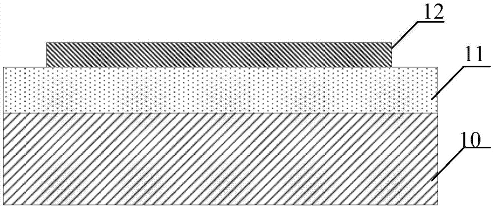
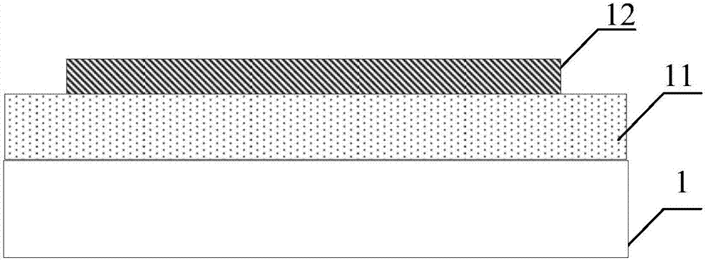
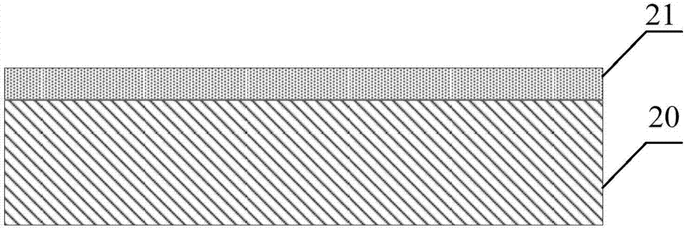
[0047] Please refer to the attached Figure 1-16 As shown, the present invention provides a kind of device structure preparation method using graphene as contact electrode, and the specific implementation method is as follows:
[0048] Step 1, forming a polypropylene carbonate PPC film 11 on the first substrate 10; PPC is coated on the first substrate 10 at 1500r / min with a glue leveler, and heated at 120 degrees for 3-5min until it is cured to form a film; then a mechanically peeled first h-BN film 12 is formed on the PPC film. A PPC-h-BN structure on the first substrate is formed. see figure 1 shown.
[0049] In step 2, peel off the PPC-h-BN structure on the first substrate 10 and place it on the PDMS film 1 to form a PDMS-PPC-h-BN structure. The surface of the PDMS film 1 and the PPC film is smooth and elastic. Since the PDMS film is relatively thick, it plays a supporting role in the subsequent dry transfer process and can be well adhered to the PPC film by van der Wa...
Embodiment 2
[0065] The present invention also provides another device structure preparation method using graphene as a contact electrode, which at least includes the steps:
[0066] a) see Figure 17 As shown, a polypropylene carbonate PPC film 11' is formed on the first substrate 10'; PPC is coated on the first substrate 10' at 1500r / min with a glue leveler, and heated at 120 degrees for 3 -5min until solidified into a film; then form a mechanically peeled h-BN film 12' on the PPC film 11';
[0067] b) Peel off the PPC-h-BN on the first substrate 10', and put it on the PDMS elastic film 1' with support and adhesion, please refer to the attached Figure 18 shown.
[0068] c) MoS is formed on the second substrate 30' 2 Film 31'; see Figure 19 shown.
[0069] d) Adsorption of MoS in step c) with the PDMS-PPC-h-BN structure 2 thin film; obtain PDMS—PPC—h-BN—MoS 2 structure; see Figure 20 and Figure 21 shown.
[0070] e) see Figure 22 and 23 As shown, a graphene film 21' is fo...
PUM
 Abstract
Description
Claims
Application Information
 - Generate Ideas
- Intellectual Property
- Life Sciences
- Materials
- Tech Scout
- Unparalleled Data Quality
- Higher Quality Content
- 60% Fewer Hallucinations
Browse by: Latest US Patents, China's latest patents, Technical Efficacy Thesaurus, Application Domain, Technology Topic, Popular Technical Reports.
© 2025 PatSnap. All rights reserved.Legal|Privacy policy|Modern Slavery Act Transparency Statement|Sitemap|About US| Contact US: help@patsnap.com


