A kind of flexible tactile sensor with multi-layer structure and its manufacturing method
A tactile sensor, multi-layer structure technology, applied in the direction of instruments, piezoelectric/electrostrictive/magnetostrictive devices, measuring force, etc., can solve the problems of easy generation of gaps in the electrode layer and low sensitivity, and achieve good extensibility , good adhesion strength, and the effect of preventing cracks
- Summary
- Abstract
- Description
- Claims
- Application Information
AI Technical Summary
Problems solved by technology
Method used
Image

Examples
preparation example Construction
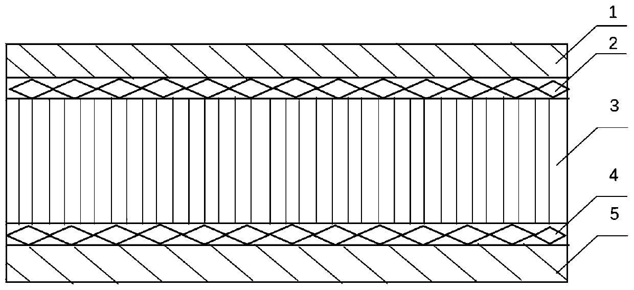
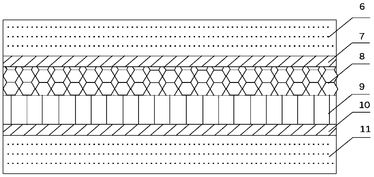
[0017] A kind of flexible tactile sensor preparation method of multilayer structure of the present invention comprises the following steps:
[0018] 1. Preparation of Ag electrodes;
[0019] 2. Preparation of PDMS film;
[0020] 3. Preparation of AuNPs-PDMS thin film;
[0021] 4. Preparation of PI film;
[0022] 5. Assemble the capacitive sensor.
Embodiment 1
[0024] 1. Manufacture the upper and lower capacitor electrodes through the magnetron sputtering process; 1: At room temperature, turn on the power supply, open the inflation valve, open the cavity to place the PET film, close the cavity, and close the inflation valve. The target used is a silver target. Two: Turn on the vacuum gauge, mechanical pump, and solenoid valve to pump for 30 seconds, turn on the molecular pump, and turn off the solenoid valve. Turn on the circulating water, open the V1 valve to pump to below 20Pa, open the Ar valve, pump to below 4.0Pa, and close the V1 valve. Three: Open the Ar cylinder and switch the molecular pump. Turn off the vacuum gauge, turn on the flow display, and adjust the valve control to 14 sccm. Four: Close the small G valve, adjust the pressure: 2.2Pa, open the target baffle. Turn on the RF power, turn on the stepping electrodes, and go forward. Five: Pre-sputter for 2 minutes, wait for the parameters to stabilize, adjust the G valv...
Embodiment 2
[0030] 1. Manufacture the upper and lower capacitor electrodes through the magnetron sputtering process; 1: At room temperature, turn on the power supply, open the inflation valve, open the cavity to place the PET film, close the cavity, and close the inflation valve. Two: Turn on the vacuum gauge, mechanical pump, and solenoid valve to pump for 30 seconds, turn on the molecular pump, and turn off the solenoid valve. Turn on the circulating water, open the V1 valve to pump to below 20Pa, open the Ar valve, pump to below 4.0Pa, and close the V1 valve. Three: Open the Ar cylinder and switch the molecular pump. Turn off the vacuum gauge, turn on the flow display, and adjust the valve control to 14 sccm. Four: Close the small G valve, adjust the pressure: 2.2Pa, open the target baffle. Turn on the RF power, turn on the stepping electrodes, and go forward. Five: Pre-sputter for 2 minutes, wait for the parameters to stabilize, adjust the G valve, the pressure: 0.5Pa. Non-magnetr...
PUM
| Property | Measurement | Unit |
|---|---|---|
| thickness | aaaaa | aaaaa |
| thickness | aaaaa | aaaaa |
| concentration | aaaaa | aaaaa |
Abstract
Description
Claims
Application Information
 - Generate Ideas
- Intellectual Property
- Life Sciences
- Materials
- Tech Scout
- Unparalleled Data Quality
- Higher Quality Content
- 60% Fewer Hallucinations
Browse by: Latest US Patents, China's latest patents, Technical Efficacy Thesaurus, Application Domain, Technology Topic, Popular Technical Reports.
© 2025 PatSnap. All rights reserved.Legal|Privacy policy|Modern Slavery Act Transparency Statement|Sitemap|About US| Contact US: help@patsnap.com