Composite substrate, composite film and preparation method thereof, and radio frequency surface acoustic wave device

A composite substrate and composite thin film technology, applied in the direction of electrical components, impedance networks, etc., can solve the problems of chemical bond breaking between layers, falling off, insufficient carrier trap density, etc.

Pending Publication Date: 2021-04-16
JINAN JINGZHENG ELECTRONICS
View PDF5 Cites 1 Cited by
  • Summary
  • Abstract
  • Description
  • Claims
  • Application Information

AI Technical Summary

Problems solved by technology

[0005] The application provides a composite substrate, a composite thin film and its preparation method, and a radio frequency surface acoustic wave device to solve the problem of insufficient carrier trap density in the prior art, which may lead to limited sound velocity difference and chemical bonds at the interface of high sound velocity trap layers. Interlayer gaps due to fracture, or even the problem of high-sonic trap layers falling off the semiconductor substrate layer directly

Method used


Image

  • Composite substrate, composite film and preparation method thereof, and radio frequency surface acoustic wave device
  • Composite substrate, composite film and preparation method thereof, and radio frequency surface acoustic wave device
  • Composite substrate, composite film and preparation method thereof, and radio frequency surface acoustic wave device

Examples


preparation example Construction

[0046] The embodiment part of the present application also provides a kind of preparation method of composite film, specifically, such as Figure 4 Shown, preparation method comprises the following steps:

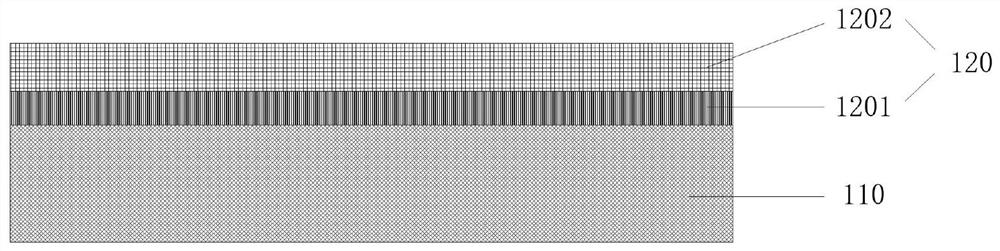
[0047] Step S11 , cleaning the substrate layer 110 to obtain the substrate layer 110 with a clean surface.

[0048] Optionally, in this step, the substrate layer 110 uses the RCA wet chemical cleaning method to remove particle contamination and some metal impurities on the substrate layer 110. The material of the substrate layer 110 can be silicon, lithium niobate, lithium tantalate, quartz, sapphire, Silicon carbide, etc., and the material of the substrate layer 110 can be selected according to needs, and this step is not specifically limited.

[0049] Step S12, placing the substrate layer with a clean surface in a deposition furnace and heating it to a first temperature, which is lower than the growth temperature of columnar structure crystals.

[0050] Optionally, in t...

Embodiment 1

[0067] Embodiment 1 (ion implantation method is combined with bonding separation method)

[0068] 1) Prepare the single crystal silicon substrate and clean it by RCA wet chemical cleaning method.

[0069] 2) The single crystal silicon substrate cleaned in step 1) is placed in a low-pressure vapor deposition furnace and heated to 580°C.

[0070] 3) Pass SiH 4 At the same time, increase the growth temperature to 625°C at a rate of 10°C / min to obtain a grain gradient layer with a thickness of 50nm. The grains in the grain gradient layer grow from the maximum width of less than 30nm to columnar grains, forming uniform grains. layer.

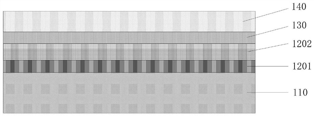
[0071] 4) growing silicon dioxide on the uniform layer of crystal grains, and grinding and polishing the grown silicon dioxide to form an isolation layer.

[0072] 5) Prepare a lithium niobate wafer with the same size as the single crystal silicon substrate, and implant helium ions (He+) into the lithium niobate wafer by ion implantation. The impl...

Embodiment 2

[0076] Embodiment 2 (bonding method is combined grinding and polishing method)

[0077] 1) Prepare the single crystal silicon substrate and clean it by RCA wet chemical cleaning method.

[0078] 2) The single crystal silicon substrate cleaned in step 1) is placed in a low-pressure vapor deposition furnace and heated to 500°C.

[0079] 3) Pass SiH 4 Gas, while increasing the growth temperature to 625°C at a rate of 5°C / min to obtain a grain-graded layer with a thickness of 200nm. The grain-graded layer grows from amorphous silicon to polysilicon containing columnar grains.

[0080] 4) growing silicon dioxide on the uniform layer of crystal grains, and grinding and polishing the grown silicon dioxide to form an isolation layer.

[0081] 5) Prepare a lithium niobate wafer of the same size as the single crystal silicon substrate, clean the process surface, and use the method of plasma bonding to bond the process surface of the cleaned lithium niobate wafer to the second prepared...


PUM

PropertyMeasurementUnit
thicknessaaaaaaaaaa

Abstract

The invention provides a composite substrate, a composite film, a preparation method of the composite film and a radio frequency surface acoustic wave device. The composite substrate sequentially comprises a substrate layer and a polycrystalline layer from bottom to top, wherein the polycrystalline layer comprises a crystal grain gradient layer and a crystal grain uniform layer; crystal grains in the crystal grain gradient layer are of a columnar structure, and the crystal grains of the columnar structure are gradually increased in the direction from the substrate layer to the crystal grain uniform layer. The grain gradient layer grows on the substrate layer, columnar grains in the grain gradient layer are sufficient in density, meanwhile, large stress generated after high-temperature cooling of the grain uniform layer can be dispersed, and interlayer gaps generated by chemical bond breakage due to the fact that the large stress acts on the substrate layer and the grain uniform layer are avoided; the surface, close to the substrate layer, of the crystal grain uniform layer is provided with dense carrier traps, and the effect of limiting carrier movement is enhanced, so that the interface resistivity is improved, the radio frequency loss of the radio frequency surface acoustic wave device is reduced, and the performance of the radio frequency surface acoustic wave device is improved.

Description

technical field [0001] The present application relates to the field of semiconductor technology, in particular to a composite substrate, a composite thin film and a preparation method thereof, and a radio frequency surface acoustic wave device. Background technique [0002] At present, the processing technology of silicon materials is very mature, and it is also a semiconductor material with more industrial applications. Therefore, silicon materials have been widely used in electronic components. Since the silicon material itself has a centrosymmetric crystal structure, silicon has no linear piezoelectric effect. Therefore, the silicon material cannot be directly used to prepare high-performance radio frequency surface acoustic wave devices. [0003] The performance of RF surface acoustic wave devices depends on the good piezoelectric properties of composite piezoelectric substrates. The main structure of the composite piezoelectric substrate includes a piezoelectric layer,...

Claims


Application Information

Patent Timeline
Patent Type & Authority Applications(China)
IPC IPC(8): H03H3/02H03H9/02H03H9/17
Inventor 李真宇杨超李洋洋张秀全刘阿龙韩智勇
Owner JINAN JINGZHENG ELECTRONICS
Why Eureka
Try Eureka