Low-loss gallium nitride radio frequency material epitaxial structure and preparation method

An epitaxial structure, gallium nitride technology, applied in semiconductor/solid-state device manufacturing, electrical components, circuits, etc., can solve problems such as increased resistance and reduced concentration of two-dimensional electron gas

Pending Publication Date: 2021-03-19
DONGGUAN INST OF OPTO ELECTRONICS PEKING UNIV
View PDF14 Cites 0 Cited by
  • Summary
  • Abstract
  • Description
  • Claims
  • Application Information

AI Technical Summary

Problems solved by technology

[0004] In order to solve the above problems, the present invention provides a low-loss GaN radio-frequency material epitaxial structure and preparation method, which mainly solves the problem that the on-resistance increases due to the decrease in the concentration of two-dimensional electron gas of GaN radio-frequency materials under high-frequency conditions. phenomenon, ultimately reducing RF loss and achieving high-quality RF dynamic device characteristics

Method used


Image

  • Low-loss gallium nitride radio frequency material epitaxial structure and preparation method
  • Low-loss gallium nitride radio frequency material epitaxial structure and preparation method
  • Low-loss gallium nitride radio frequency material epitaxial structure and preparation method

Examples


preparation example Construction

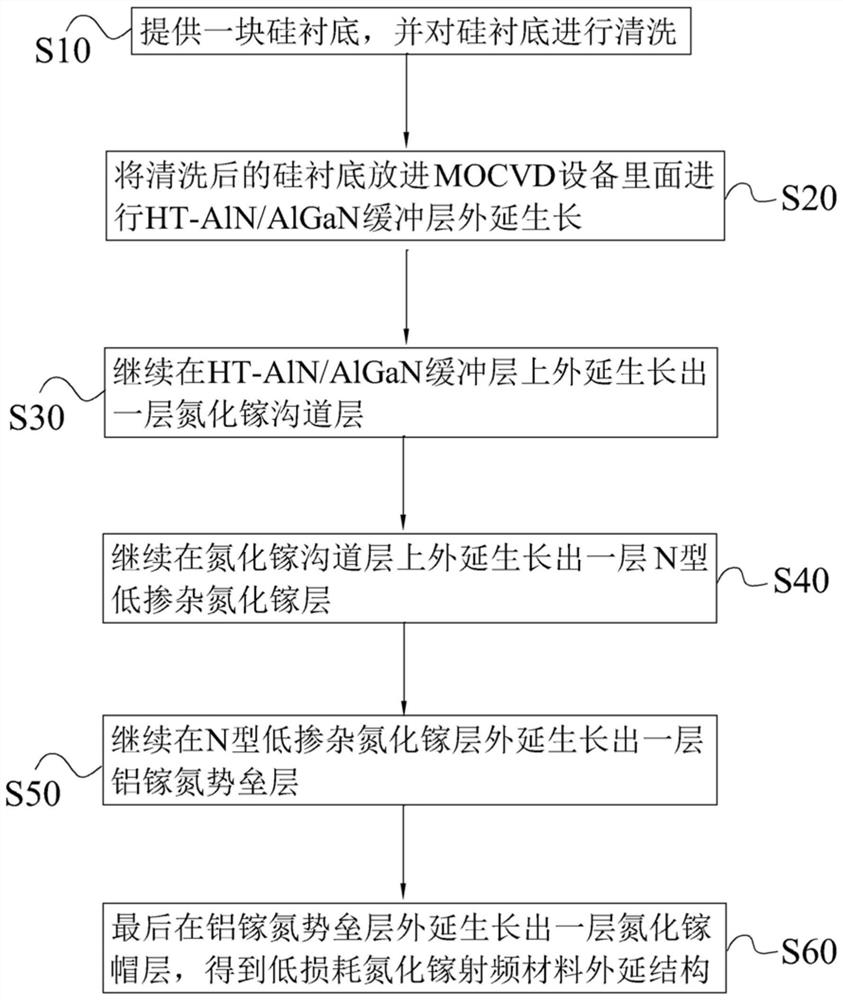
[0046] see figure 2 As shown, the present invention relates to a method for preparing a low-loss gallium nitride radio frequency material epitaxial structure, comprising the following steps:

[0047] S10, providing a silicon substrate, and cleaning the silicon substrate;

[0048] S20, putting the cleaned silicon substrate into the MOCVD equipment for epitaxial growth of the HT-AlN / AlGaN buffer layer;

[0049] S30, continuing to epitaxially grow a gallium nitride channel layer on the HT-AlN / AlGaN buffer layer;

[0050] S40, continuing to epitaxially grow an N-type low-doped GaN layer on the GaN channel layer;

[0051] S50, continuing to epitaxially grow an AlGaN barrier layer on the N-type low-doped GaN layer;

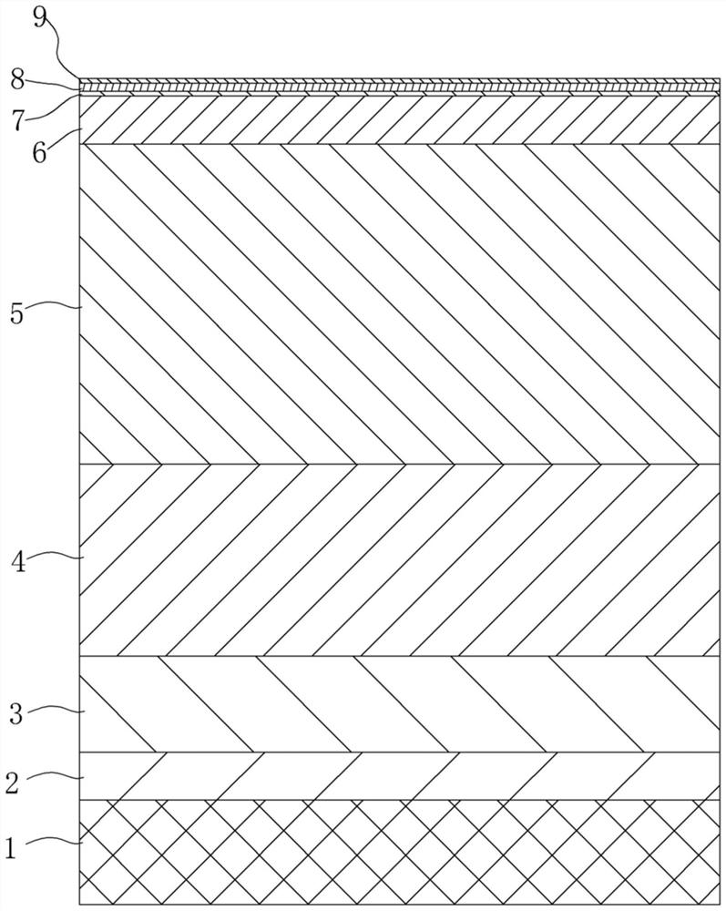
[0052] S60. Finally, a GaN cap layer is epitaxially grown on the AlGaN barrier layer to obtain a low-loss GaN radio frequency material epitaxial structure.

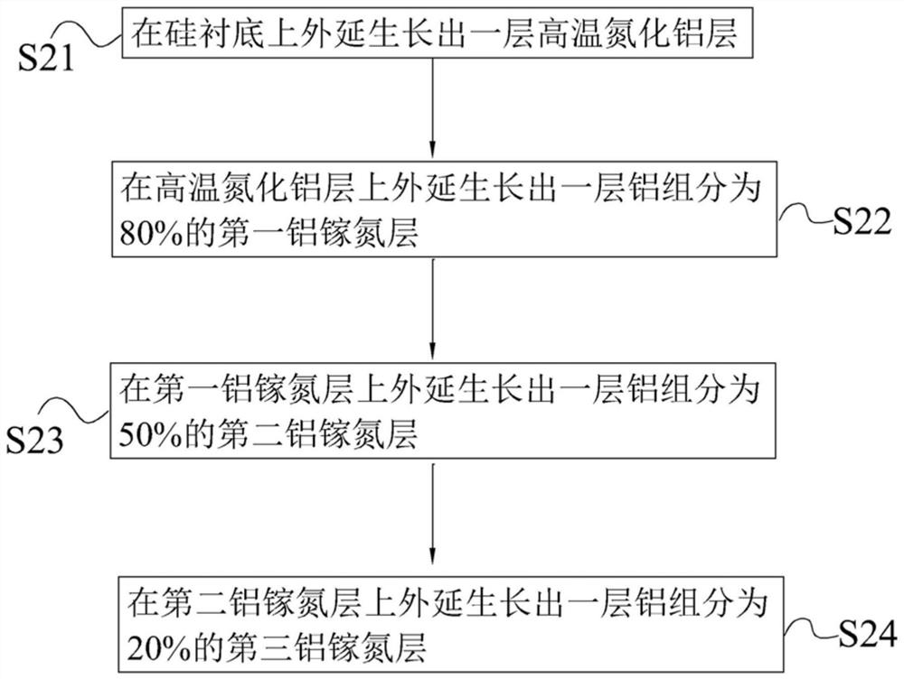
[0053] Such as image 3 As shown, in step S20, the steps of epitaxial growth of the HT-AlN / AlGaN buffer laye...


PUM

PropertyMeasurementUnit
Thicknessaaaaaaaaaa
Thicknessaaaaaaaaaa
Thicknessaaaaaaaaaa

Abstract

The invention relates to the technical field of semiconductors, in particular to a low-loss gallium nitride radio frequency material epitaxial structure and a preparation method. A buffer layer, a gallium nitride channel layer, an N-type low-doped gallium nitride layer, a barrier layer and an amide cap layer epitaxially grow on a silicon substrate in sequence to obtain the low-loss gallium nitrideradio frequency material epitaxial structure. According to the invention, the N-type low-doped gallium nitride layer is added below the barrier layer, and the square resistance of the N-type low-doped gallium nitride layer is lower than that of two-dimensional electron gas, so that the N-type low-doped gallium nitride layer has a very weak function of participating in conduction under a normal on-state condition, but in the process from an off state to an on stage, electrons of the N-type low-doped gallium nitride layer can supplement the reduction of the concentration of two-dimensional electron gas; secondly, electrons transferred back to a heterojunction interface from the buffer layer can quickly pass through the N-type low-doped gallium nitride layer, so that the effect of quickly supplementing two-dimensional electron gas of the heterojunction interface is achieved; and therefore, the concentration of the two-dimensional electron gas in the dynamic process can be reduced to themaximum extent by adding the N-type low-doped gallium nitride layer, so that the radio frequency loss is reduced.

Description

technical field [0001] The invention relates to the technical field of semiconductors, in particular to a low-loss gallium nitride radio-frequency material epitaxial structure and a preparation method. Background technique [0002] The third-generation semiconductors have excellent properties such as high band gap, high breakdown electric field, high saturation electron drift velocity, and strong polarization. Among them, compared with traditional Si materials and other devices, GaN-based devices have higher power density output, higher strong field, and lower on-resistance, so GaN-based devices have higher energy in practical applications. Conversion frequency efficiency and output power, due to its excellent performance, it is widely used in consumer electronics, 5G communications, cloud services, photovoltaic inverters, new energy vehicles, power generation and other fields. [0003] In recent years, the commercialization progress of GaN epitaxial materials and devices o...

Claims


Application Information

Patent Timeline
IPC IPC(8): H01L29/06H01L29/778H01L21/335
CPCH01L29/0684H01L29/66462H01L29/7783
Inventor 王琦梁智文王新强张国义
Owner DONGGUAN INST OF OPTO ELECTRONICS PEKING UNIV
Why Eureka
Try Eureka