Antifuse structure circuit and method of forming same

An anti-fuse and circuit technology, applied in circuits, electrical components, electrical solid devices, etc., can solve the problems of poor anti-fuse structure and performance, and achieve the effects of large breakdown current, improved integration, and sufficient breakdown.

Active Publication Date: 2020-05-08
SEMICON MFG INT (SHANGHAI) CORP +1
View PDF3 Cites 0 Cited by
  • Summary
  • Abstract
  • Description
  • Claims
  • Application Information

AI Technical Summary

Problems solved by technology

[0004] However, existing antifuse structures perform poorly

Method used


Image

  • Antifuse structure circuit and method of forming same
  • Antifuse structure circuit and method of forming same
  • Antifuse structure circuit and method of forming same

Examples


Embodiment Construction

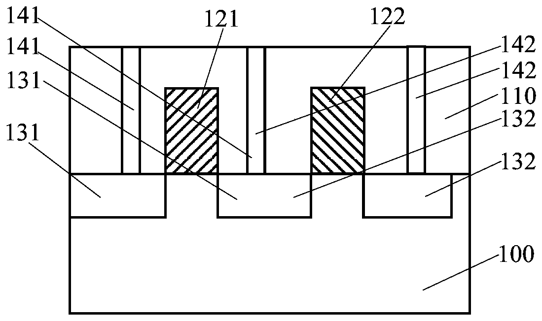
[0031] As mentioned in the background, the performance of existing antifuse structure circuits is poor.

[0032] refer to figure 1, the antifuse structure circuit includes: a substrate 100; a control gate structure group located on the substrate 100 and a dielectric layer 110 covering the control gate structure group, and the control gate structure group includes a first gate structure 121 and a second gate structure group Gate structure 122; first source-drain doped regions 131 respectively located in the substrate 100 on both sides of the first gate structure 121; second source-drain doped regions 132 respectively located in the substrate 100 on both sides of the second gate structure 122 , the first gate structure 121 and the second gate structure 122 share the source and drain; the first conductive plug 141 located on the first source-drain doped region 131 and electrically connected to the first source-drain doped region 131; The second conductive plug 142 on the second ...


PUM


Abstract

The invention relates to an anti-fuse structural circuit and a formation method thereof. The anti-fuse structural circuit comprises a substrate comprising a control area, a control grid structure group located on the control area of the substrate, an antifuse, a first conductive plug and a second conductive plug, wherein the control grid structure group comprises a first grid structure; the antifuse comprises an interlayer dielectric layer which is located on the substrate and covers the first grid structure, the interlayer dielectric layer comprises a first dielectric layer, and the top surface of the first dielectric layer is flushed with the top surface of the first grid structure; the first conductive plug penetrates the interlayer dielectric layer of the first grid structure and covers the top surface of the first grid structure and partial first dielectric layer at the two sides of the first grid structure; and the second conductive plug penetrates the interlayer dielectric layerat the two sides of the first grid structure, a first distance is kept between the second conductive plug and the first conductive plug, a second distance is kept between the second conductive plug and the first grid structure, and the first distance is smaller than the second distance. The performance of the anti-fuse structural circuit is improved.

Description

technical field [0001] The invention relates to the field of semiconductor manufacturing, in particular to an antifuse structure circuit and a forming method thereof. Background technique [0002] In the semiconductor industry, fuse elements are widely used in integrated circuits due to their multiple uses. For example, multiple circuit modules with the same function are designed in the integrated circuit as a backup. When one of the circuit modules is found to be invalid, the circuit module and other functional circuits in the integrated circuit are blown through the fuse element, and the circuit module with the same function is used. Another circuit module replaces the failed circuit module. [0003] With the continuous development of semiconductor technology, anti-fuse (Anti-fuse) technology has attracted the attention of many inventors and manufacturers. An antifuse structure is a structure that can change the conduction state. The antifuse structure is non-conductive...

Claims


Application Information

Patent Timeline
Patent Type & Authority Patents(China)
IPC IPC(8): H01L23/525H01L23/528H01L21/60
CPCH01L23/5252H01L23/528H01L24/03H01L2224/03
Inventor 冯军宏甘正浩
Owner SEMICON MFG INT (SHANGHAI) CORP
Why Eureka
Try Eureka