Rare earth electrogenerated dark blue light device
An optical device, dark blue technology, applied in the direction of electric solid devices, electrical components, semiconductor devices, etc., can solve the problems of blue color distortion, easy aging, poor stability of OLED, etc., to achieve high mobility, not easy to aging, good stability Effect
- Summary
- Abstract
- Description
- Claims
- Application Information
AI Technical Summary
Problems solved by technology
Method used
Image
Examples
Embodiment 1
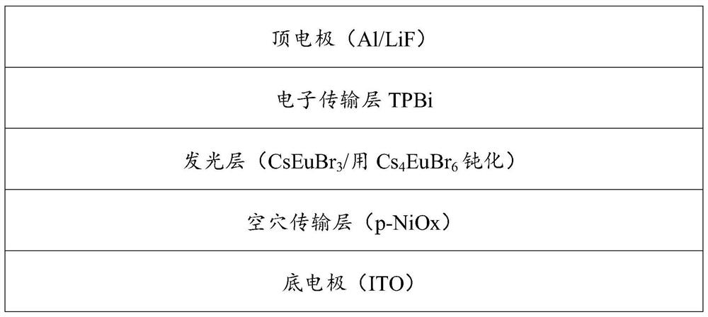
[0038] In this embodiment, the light-emitting layer material is passivated CsEuBr 3 Taking an electroluminescent blue light device as an example, its specific preparation method includes the following steps:
[0039] a) Use detergent, deionized water, acetone and absolute ethanol to ultrasonically clean the substrate ITO in sequence, for half an hour each time; where, ITO uses a substrate that has been etched two times, and its light-emitting area is about 2mm*2mm;
[0040] b) Using magnetron sputtering method on ITO, sputtering Li-doped p-type NiO with a thickness of about 40nm, wherein the doping concentration is 10 16 -10 17 cm -3 ;
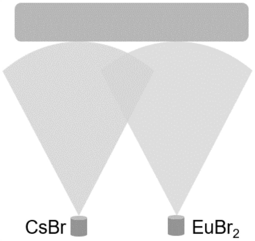
[0041] c) Put the substrate coated with NiO film into the evaporation glove box, and pump the vacuum to 4*10 -5 Below Pa, the substrate is heated to 200°C, and EuBr is evaporated at a speed of 0.11nm / s by co-evaporation 2 , CsBr was evaporated at a speed of 0.14nm / s, with a total thickness of 100nm. In the dual-source co-evaporation proc...
Embodiment 2
[0051] In this embodiment, the light-emitting layer material is passivated CsEuBr 3 Taking an electroluminescent blue light device as an example, its specific preparation method includes the following steps:
[0052] a) Use detergent, deionized water, acetone and absolute ethanol to ultrasonically clean the substrate ITO in sequence, for half an hour each time; where, ITO uses a substrate that has been etched two times, and its light-emitting area is about 2mm*2mm;
[0053] b) Using magnetron sputtering method on ITO, sputtering Li-doped p-type NiO with a thickness of about 40nm, wherein the doping concentration is 10 16 -10 17 cm -3 ;
[0054] c) Put the substrate coated with NiO film into the evaporation glove box, and pump the vacuum to 4*10 -5 Below Pa, the substrate is heated to 200°C, and EuBr is evaporated at a speed of 0.12nm / s by co-evaporation 2 , CsBr was vapor-deposited at a speed of 0.18nm / s, and a total thickness of 100nm was vapor-deposited.
[0055] d) Ta...
Embodiment 3
[0058] In this embodiment, the light-emitting layer material is passivated CsEuBr 3 Taking an electroluminescent blue light device as an example, its specific preparation method includes the following steps:
[0059] a) Use detergent, deionized water, acetone and absolute ethanol to ultrasonically clean the substrate ITO in sequence, for half an hour each time; where, ITO uses a substrate that has been etched two times, and its light-emitting area is about 2mm*2mm;
[0060] b) Using magnetron sputtering method on ITO, sputtering Li-doped p-type NiO with a thickness of about 40nm, wherein the doping concentration is 10 16 -10 17 cm -3 ;
[0061] c) Put the substrate coated with NiO film into the evaporation glove box, and pump the vacuum to 4*10 -5 Below Pa, the substrate is heated to 200°C, and EuBr is evaporated at a speed of 0.115nm / s by co-evaporation 2 , CsBr was evaporated at a speed of 0.16nm / s, and a total thickness of 100nm was evaporated.
[0062] d) Take the sh...
PUM
| Property | Measurement | Unit |
|---|---|---|
| electron mobility | aaaaa | aaaaa |
| hole mobility | aaaaa | aaaaa |
Abstract
Description
Claims
Application Information
 - R&D
- Intellectual Property
- Life Sciences
- Materials
- Tech Scout
- Unparalleled Data Quality
- Higher Quality Content
- 60% Fewer Hallucinations
Browse by: Latest US Patents, China's latest patents, Technical Efficacy Thesaurus, Application Domain, Technology Topic, Popular Technical Reports.
© 2025 PatSnap. All rights reserved.Legal|Privacy policy|Modern Slavery Act Transparency Statement|Sitemap|About US| Contact US: help@patsnap.com


