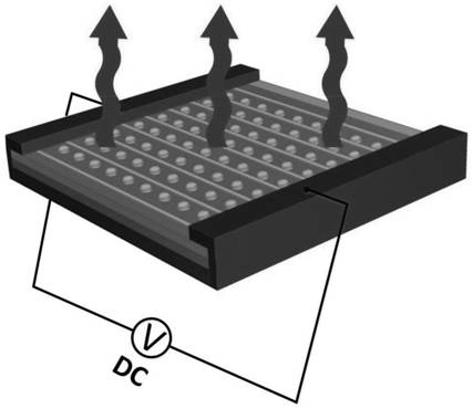
Manufacturing method of embedded self-demisting and zooming micro-lens array, product manufactured by using method, and application of product
A microlens array and embedded technology, which is applied in the fields of lens, processing and manufacturing, and manufacturing tools, can solve problems such as difficult to achieve fast zooming, fogging, and frosting, and achieve excellent microlens defogging and zooming performance, while reducing production costs. Low, the effect of reducing manufacturing costs
- Summary
- Abstract
- Description
- Claims
- Application Information
AI Technical Summary
Problems solved by technology
Method used
Image
Examples
Embodiment 1
[0044] Step 1: Prepare the printing substrate
[0045] (1) Choose ordinary glass as the hard substrate, first place the ordinary glass in isopropanol solution for ultrasonic cleaning for 5 minutes, then place it in deionized water for ultrasonic cleaning for 5 minutes, and finally dry it with nitrogen, take it out for use;
[0046] (2) The PDMS liquid is Sylgard 184 from Dow Corning Company, and the PDMS elastomer and its corresponding curing agent are stirred and mixed evenly at a mass ratio of 10:1, and placed in a vacuum drying oven to evacuate to remove air bubbles;
[0047] (3) Pour the vacuum-treated PDMS liquid on the surface of ordinary glass, let it stand for 2 minutes, and then place it on a coater for spin coating. The spin coating time is 2 minutes, and the rotation speed is 500r / min to form a layer of PDMS liquid about 50 μm thick. Finally, place it in a vacuum drying oven and heat it at 70°C for 30 minutes, the PDMS will be cross-linked and cured by heating, and ...
Embodiment 2
[0056] Step 1: Prepare the printing substrate
[0057] (1) Choose a silicon wafer as the hard substrate, first clean the silicon wafer with isopropanol solution for 5 minutes, then place it in deionized water for 5 minutes to remove the residual isopropanol solution, and finally dry it with nitrogen, take it out for use ;
[0058] (2) Select Sylgard 184 from Dow Corning as the PDMS liquid, stir and mix the PDMS elastomer and curing agent at a ratio of 10:1, and place in a vacuum drying oven to evacuate to remove air bubbles;
[0059] (3) Pour the vacuum-treated PDMS liquid on the surface of the silicon wafer, spin-coat it with a coating machine, spin-coat for 2 minutes, and rotate at a speed of 500r / min to form a layer of PDMS liquid about 50 μm thick; finally place it in vacuum drying Heating in the box at 75°C for 30 minutes, the PDMS is heated to cross-link and solidify, and the printing substrate is prepared;
[0060] Step 2: Print Microlens Array
[0061] (1) Select 60...
Embodiment 3
[0071] Step 1: Prepare the printing substrate.
[0072] (1) Select high-quality float glass as the hard substrate, first place the float glass in isopropanol solution for ultrasonic cleaning for 5 minutes, then place it in deionized water for ultrasonic cleaning for 5 minutes, and finally dry it with nitrogen, take it out for use;
[0073] (2) The PDMS liquid is Sylgard 184 from Dow Corning Company. The PDMS elastomer and its corresponding curing agent are stirred and mixed evenly at a ratio of 10:1, and placed in a vacuum drying oven to evacuate to remove air bubbles;
[0074] (3) Pour the vacuum-treated PDMS liquid on the surface of the float glass, let it stand for 2 minutes, and then place it on a homogenizer for spin coating. The spin coating time is 1 min, and the speed is 500r / min to form a layer of PDMS liquid about 80 μm thick. . Finally, it was placed in a vacuum drying oven and heated at 75°C for 30 minutes. The PDMS was heated to cross-link and solidify, and the pri...
PUM
| Property | Measurement | Unit |
|---|---|---|
| Viscosity | aaaaa | aaaaa |
| The inside diameter of | aaaaa | aaaaa |
| The inside diameter of | aaaaa | aaaaa |
Abstract
Description
Claims
Application Information
 - R&D Engineer
- R&D Manager
- IP Professional
- Industry Leading Data Capabilities
- Powerful AI technology
- Patent DNA Extraction
Browse by: Latest US Patents, China's latest patents, Technical Efficacy Thesaurus, Application Domain, Technology Topic, Popular Technical Reports.
© 2024 PatSnap. All rights reserved.Legal|Privacy policy|Modern Slavery Act Transparency Statement|Sitemap|About US| Contact US: help@patsnap.com


