Nano rod-shaped antimony trisulfide electromagnetic wave absorbing material, absorber, preparation method and application

A nano-rod-shaped antimony trisulfide technology, which is applied in chemical instruments and methods, polycrystalline material growth, electrical components, etc., can solve the problems of increasing the reflection of electromagnetic waves by materials, reducing the efficiency of electromagnetic wave absorption, and insufficient loss capacity, etc., to achieve Unique microscopic morphology, improved bulk polarization relaxation loss capability, and improved polarization characteristics

Active Publication Date: 2021-09-03
SHANDONG UNIV
View PDF0 Cites 0 Cited by
  • Summary
  • Abstract
  • Description
  • Claims
  • Application Information

AI Technical Summary

Problems solved by technology

Although dielectric absorbing materials have been studied in depth, the inventors believe that they still have inherent performance defects: high-loss carbon materials and conductive high polymers will cause high dielectric loss due to their high electrical conductivity. However, the impedance mismatch increases the material’s reflection of electromagnetic waves; while metal oxides or sulfides can maintain good impedance matching characteristics, but their loss capability is insufficient, which will eventually reduce the material’s absorption efficiency of electromagnetic waves.
On the other hand, many current methods for preparing electromagnetic wave absorbing materials with high efficiency, such as liquid phase exchange method, vapor phase deposition method, etc., are expensive and cumbersome to operate, and mainly stay in the laboratory research stage.

Method used


Image

  • Nano rod-shaped antimony trisulfide electromagnetic wave absorbing material, absorber, preparation method and application
  • Nano rod-shaped antimony trisulfide electromagnetic wave absorbing material, absorber, preparation method and application
  • Nano rod-shaped antimony trisulfide electromagnetic wave absorbing material, absorber, preparation method and application

Examples


preparation example Construction

[0039] In a third aspect, the present invention provides a method for preparing the nanorod-shaped antimony trisulfide electromagnetic wave absorbing material, comprising the following steps:

[0040] Solvothermal reaction of mixed solution of antimony source and sulfur source to prepare nanorod-like Sb 2 S 3 Electromagnetic wave absorbing materials;

[0041] The antimony source is antimony chloride (SbCl 3 ), antimony nitrate (Sb(NO 3 ) 3 ) or antimony acetate (Sb(CH 3 COO) 3 ) in any one or a mixture of two or more;

[0042] The sulfur source is sodium sulfide (Na 2 S), potassium sulfide (K 2 S), thioacetamide (C 3 h 7 NO 2 S) or L-cysteine ​​(C 3 h 7 NO 2 S).

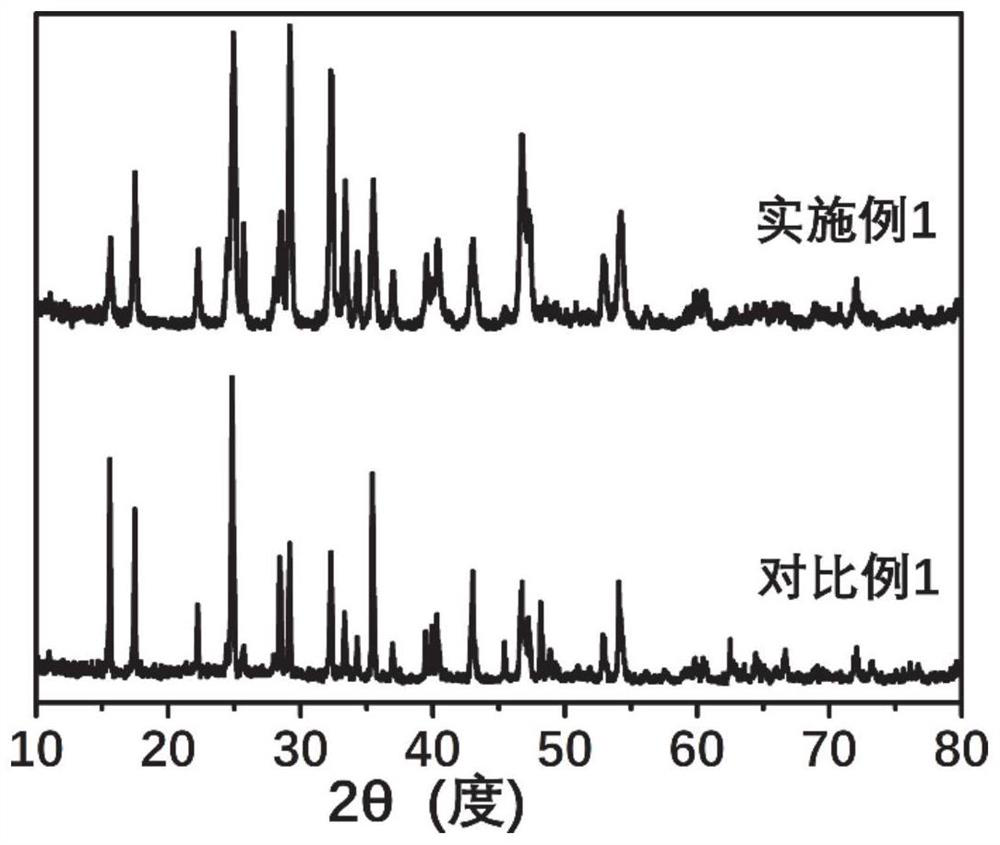
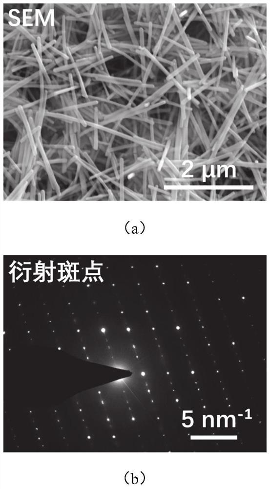
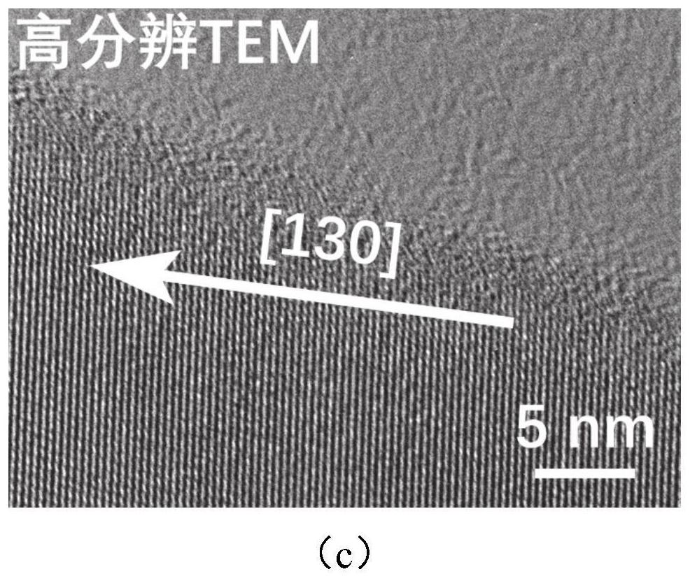
[0043] This preparation method utilizes a special sulfur source as a reactant and a surfactant to regulate the solution surface properties of the reaction environment at the same time, so that Sb 2 S 3 In the process of formation and growth, the [130] direction is the preferential growth direction of...

Embodiment 1

[0052] A nanorod-like Sb 2 S 3 The preparation method of the filled electromagnetic wave absorber comprises the following steps:

[0053] (1) 2.5mmol SbCl 3 , 5.0 mmol C 3 h 7 NO 2 S and 5.0 mmol Na 2 S was successively dissolved in 50.0 mL of deionized water and stirred continuously for 3 h until a homogeneous solution was obtained.

[0054] (2) Transfer all the solution in step (1) to a polytetrafluoroethylene-lined steel reaction kettle, and heat to 200° C. for 2 h. The obtained solid product was centrifuged, washed several times with ethanol / water mixture, and then dried under vacuum at 60° C. for 12 h.

[0055] (3) After the solid paraffin is melted at a temperature above 75° C., mixed with an equal mass of the solid product in step (2), stirred rapidly, cooled to room temperature, and pressed into an absorber.

Embodiment 2

[0057] A nanorod-like Sb 2 S 3 The preparation method of the filled electromagnetic wave absorber comprises the following steps:

[0058] (1) 2.5mmol Sb(CH3COO) 3 and 10.0 mmol C 3 h 7 NO 2 S was successively dissolved in 50.0 mL of deionized water and stirred continuously for 3 h until a homogeneous solution was obtained.

[0059] (2) Transfer all the solution in step (1) to a polytetrafluoroethylene-lined steel reaction kettle, and heat to 200° C. for 4 h. The obtained solid product was centrifuged, washed several times with ethanol / water mixture, and then dried under vacuum at 60° C. for 12 h.

[0060] (3) After the solid paraffin is melted at a temperature above 75° C., mixed with an equal mass of the solid product in step (2), stirred rapidly, cooled to room temperature, and pressed into an absorber.


PUM

PropertyMeasurementUnit
diameteraaaaaaaaaa
lengthaaaaaaaaaa

Abstract

The invention discloses a nano-rod-shaped antimony trisulfide electromagnetic wave absorbing material, an absorber, a preparation method and an application thereof. The nano-rod-shaped Sb 2 S 3 Electromagnetic wave absorbing materials, which are single crystal nanorods stacked interlaced, Sb 2 S 3 The crystal orientation of nanorods is [130], which is orthorhombic stibnite, Sb 2 S 3 During the crystallization process, the nanorods are grown in the [130] direction, and the prepared Sb 2 S 3 Nanorods realize Sb for the first time 2 S 3 It is applied in the field of electromagnetic wave absorption, and has the characteristics of high absorption intensity, wide absorption frequency band, thin matching thickness, strong corrosion resistance, etc., and at the same time, the preparation method of the present invention is simple and easy, low in cost, and has good industrial application prospects.

Description

technical field [0001] The invention belongs to the technical field of electromagnetic wave absorbing materials, and in particular relates to a nanorod-shaped antimony trisulfide electromagnetic wave absorbing material, absorber, preparation method and application. Background technique [0002] The information disclosed in this background section is only intended to increase the understanding of the general background of the present invention, and is not necessarily taken as an acknowledgment or any form of suggestion that the information constitutes the prior art already known to those skilled in the art. [0003] In recent years, with the rapid development of computer technology and electronic communication technology, as well as the popularization of electronic products, the increasing electromagnetic energy density will inevitably seriously pollute today's electromagnetic environment, which will not only affect the normal operation of precision electronic equipment. Inte...

Claims


Application Information

Patent Timeline
Patent Type & Authority Patents(China)
IPC IPC(8): C30B29/46C30B29/60C30B7/14H05K9/00
CPCC30B7/14C30B29/46C30B29/60H05K9/0081
Inventor 刘久荣乔靖刘伟吴莉莉王凤龙汪宙
Owner SHANDONG UNIV
Why Eureka
Try Eureka