Preparation method of all-metal organic framework Van der Waals heterojunction layer film, prepared film and application thereof

An organic framework and heterojunction technology, which is applied in the manufacture of hybrid/electric double layer capacitors, coatings, structural parts, etc., can solve problems such as difficulty, inability to prepare multilayer MOF films, and serious lattice mismatch

Active Publication Date: 2021-02-02
FUJIAN INST OF RES ON THE STRUCTURE OF MATTER CHINESE ACAD OF SCI
View PDF18 Cites 4 Cited by
  • Summary
  • Abstract
  • Description
  • Claims
  • Application Information

AI Technical Summary

Problems solved by technology

MOFs for different functions often have different unit cell parameters and topological structures, so the lattice mismatch is serious, and it is impossible to prepare high-quality multi-layer MOF thin films. The b

Method used


Image

  • Preparation method of all-metal organic framework Van der Waals heterojunction layer film, prepared film and application thereof
  • Preparation method of all-metal organic framework Van der Waals heterojunction layer film, prepared film and application thereof
  • Preparation method of all-metal organic framework Van der Waals heterojunction layer film, prepared film and application thereof

Examples


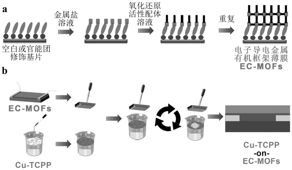
preparation example 1

[0082] The preparation of EC-MOFs thin film Cu-HHTP refers to the patent document CN 201711022911.4.

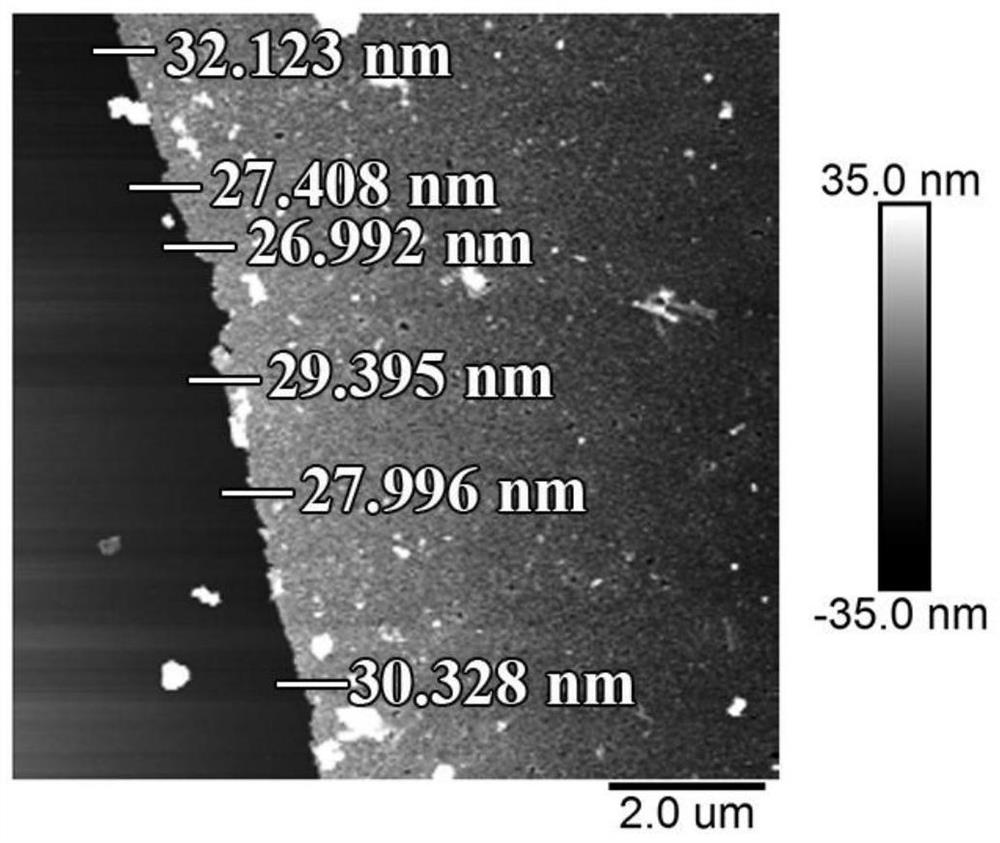
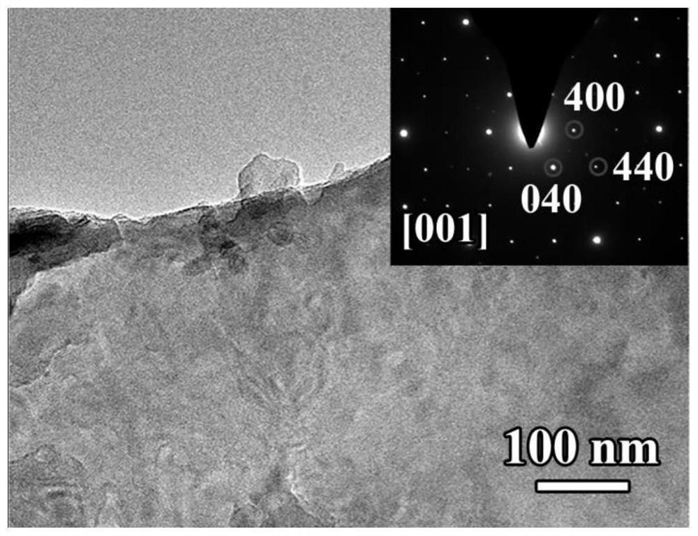
[0083] The specific preparation process is: in order to configure a solution of 0.01mM (mmol / L) copper acetate and a methanol solution of 0.01mM HHTP (2,3,6,7,10,11-hexahydroxytriphenylene), the substrate is fixed on On a substrate, layer-by-layer (Layer-by-Layer, LbL) parallel spraying is carried out. First take 3mL of copper acetate solution, spray for about 20 seconds, then rinse with 4mL of ethanol, and blow dry with nitrogen. Immediately after that, 6 mL of the methanol solution of the ligand HHTP was sprayed for about 40 seconds, followed by rinsing with 4 mL of ethanol, and drying with nitrogen gas. This is a cycle, the thickness of the film of growth is one layer, about 2nm, repeats this step 19 times, and the film of preparation is recorded as Cu-TCPP-OC-on-Cu-HHTP-20C (wherein 0C represents 0 layer, 20C represents 20 layers), the typical AFM image of the edge of t...

preparation example 2

[0085] Referring to the same method as Preparation Example 1, copper nitrate was used as a raw material, and an HHTP ligand solution was prepared with ethanol to prepare thin films Cu-HHTP-10C and Cu-HHTP-50C.

preparation example 3

[0087] Referring to the same method as Preparation Example 1, copper acetate was used as a raw material, and ethanol was used to prepare a HATP ligand solution to prepare thin films Cu-HITP-10C and Cu-HITP-50C.


PUM


Abstract

The invention provides a preparation method of an all-metal organic framework Van der Waals heterojunction layer film, the prepared film and application thereof. A MOFs Van der Waals heterojunction thin film which is controllable in thickness and uniform in homogeneity can be effectively prepared by adopting a liquid phase epitaxy/interface method and a seal/spin coating/drop coating method, and the method can be used for efficiently preparing high-quality double/multilayer MOFs Van der Waals heterojunction thin films with different functions, components and structures without the problem of lattice mismatch. The film provides a brand-new research platform for the development of thin-film electrical devices, and is expected to realize the preparation of high-performance electrical devicesthrough the functions of cascaded gas adsorption/separation, gas sensing and the like.

Description

technical field [0001] The invention relates to the field of thin film preparation, in particular to a method for preparing an all-metal organic framework van der Waals heterojunction thin film, the prepared thin film and its application. Background technique [0002] The quality and versatility of thin films is one of the important determinants of high-performance devices. Through the combination of multiple layers of different functional films, its multifunctionality and synergistic effect endow it with great potential to enhance the performance of thin film electrical devices. Therefore, multilayer thin films have attracted interest and attention from academia and industry. At the same time, exploring new multilayer functional thin films will provide a new platform for the development of electrical devices. Metal–Organic Frameworks (MOFs) are a class of crystalline porous coordination polymers with regular network structures self-assembled by metal ions or metal cluster...

Claims


Application Information

Patent Timeline
IPC IPC(8): B05D1/00B05D1/20B05D3/00B05D7/24B05D1/02B05D1/38G01N33/00G01N33/48H01M4/60H01M4/90H01M8/0202
CPCB05D1/005B05D1/20B05D3/00B05D7/24B05D1/02B05D7/584B05D7/586G01N33/0047G01N33/0062G01N33/48H01M4/606H01M4/9008H01G11/84H01M8/0202G01N2033/0068Y02E60/10Y02E60/50
Inventor 姚明水徐刚伍蔼倩
Owner FUJIAN INST OF RES ON THE STRUCTURE OF MATTER CHINESE ACAD OF SCI
Why Eureka
Try Eureka