Electromagnetic shielding module structure and preparation method of electromagnetic shielding module structure
A module structure, electromagnetic shielding technology, applied in the direction of circuits, electrical components, electric solid devices, etc., can solve the problems of poor shielding effect, difficult quality control, complex process, etc.
- Summary
- Abstract
- Description
- Claims
- Application Information
AI Technical Summary
Problems solved by technology
Method used
Image

Examples
no. 1 example
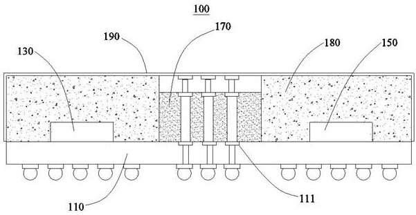
[0055] Please refer to Figure 1 to Figure 3 , this embodiment provides an electromagnetic shielding module structure 100, which avoids complex processes such as digging and filling, simplifies the process steps, reduces the difficulty of packaging, and also avoids the problem of glue overflow. The shielding device 170 is highly uniform, The sputtering of the metal layer is uniform and the shielding effect is good.
[0056] The embodiment of the present invention provides an electromagnetic shielding module structure 100, including a module substrate 110, a first chip 130, a second chip 150, a plurality of shielding devices 170, a protective plastic package 180 and a metal shielding layer 190, the first chip 130 and the second chip 150 are mounted on the module substrate 110 at intervals, a plurality of shielding devices 170 are mounted on three of the module substrate 110, and at least part of the shielding devices 170 are arranged between the first chip 130 and the second ch...
no. 2 example
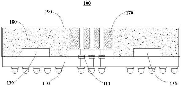
[0079] see Figure 7 , the present embodiment provides a method for preparing the electromagnetic shielding module structure 100, which is used to prepare the electromagnetic shielding module structure 100 as described in the first embodiment, the method comprising the following steps:
[0080] S1: mount the first chip 130 and the second chip 150 on the module substrate 110 .
[0081] Specifically, a module substrate 110 is provided, and the first chip 130 and the second chip 150 are mounted on the front of the module substrate 110 at intervals, and are electrically connected to the module substrate 110, and the electrical connection method may be wire bonding (front mounting ), can also be connected through solder balls (flip chip), so I won’t go into details here.
[0082] S2: Mount a plurality of shielding devices 170 on the module substrate 110 , and at least part of the shielding devices 170 are arranged between the first chip 130 and the second chip 150 .
[0083] Spec...
no. 3 example
[0115] This embodiment provides a method for preparing an electromagnetic shielding module structure 100, the basic steps of which are the same as those of the second embodiment, and where not mentioned in this embodiment can refer to the second embodiment, the method includes the following steps:
[0116] S1: mount the first chip 130 and the second chip 150 on the module substrate 110 .
[0117] S2: Mount a plurality of shielding devices 170 on the module substrate 110 , and at least part of the shielding devices 170 are arranged between the first chip 130 and the second chip 150 .
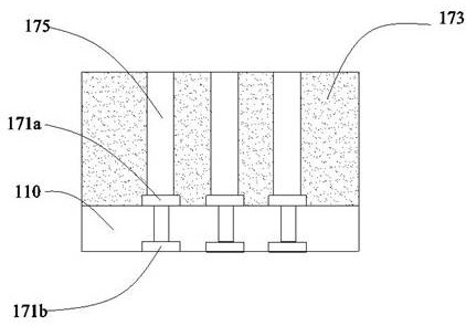
[0118] Specifically, the front side of the module substrate 110 is designed with grounding pins 111 , and the shielding device 170 is mounted on the grounding pins 111 , and the external grounding is realized through the pins on the back side of the substrate. When mounting the shielding device 170 , a front mounting structure is adopted, the shielding substrate 171 is electrically connected to t...
PUM
 Abstract
Description
Claims
Application Information
 - R&D
- Intellectual Property
- Life Sciences
- Materials
- Tech Scout
- Unparalleled Data Quality
- Higher Quality Content
- 60% Fewer Hallucinations
Browse by: Latest US Patents, China's latest patents, Technical Efficacy Thesaurus, Application Domain, Technology Topic, Popular Technical Reports.
© 2025 PatSnap. All rights reserved.Legal|Privacy policy|Modern Slavery Act Transparency Statement|Sitemap|About US| Contact US: help@patsnap.com