Lattice mismatch type three-junction gallium arsenide solar cell and manufacturing method
A technology of lattice mismatch and solar cells, applied in the field of solar cells, can solve problems such as incomplete stress release, many production steps, and long growth time, and achieve the effect of reducing product production cycle and reducing damage
- Summary
- Abstract
- Description
- Claims
- Application Information
AI Technical Summary
Problems solved by technology
Method used
Image
Examples
Embodiment 1
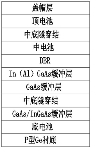
[0036] S1: On the P-type Ge substrate, at 720 ℃, by PH 3 In the form of diffusion, the bottom cell is formed emitter region, the emitter region having a thickness of 0.1 m, then the temperature was lowered to 640 deg.] C, growing GaInP nucleation layer thickness of 0.01 m, while the nucleation layer as a window layer of the bottom cell;
[0037] S2: temperature was raised to 650 ℃, the growth of GaAs / In0.01 GaAs buffer layer, GaAs with a thickness of 0.1μm, In 0.01 GaAs having a thickness of 0.1 m;
[0038] S3: temperature was lowered to 560 ℃, growth tunneling junction midsole, midsole tunneling became N ++ GaAs / P ++ GaAs structure, in which N ++ GaAs is a thickness of 0.01μm, a doping concentration of 1 × 10 19 / cm 3 , The dopant is a combination of Si and Te; P ++ GaAs is a thickness of 0.01μm, a doping concentration of 2 × 10 19 / cm 3 Dopant are C;
[0039] S4: temperature was raised to 650 ℃, the growth of GaAs buffer layer, GaAs buffer layer having a thickness of 0.2μm...
Embodiment 2
[0047] S1: On the P-type Ge substrate, at 720 ℃, by PH 3 In the form of diffusion, the bottom cell is formed emitter region, the emitter region having a thickness of 0.3 m, then the temperature was lowered to 640 deg.] C, the growth of AlGaInP nucleation layer, the thickness of 0.02 m, while the nucleation layer as a window layer of the bottom cell;
[0048] S2: temperature was raised to 650 ℃, the growth of GaAs / In 0.01 GaAs buffer layer, GaAs with a thickness of 0.1μm, In 0.01 GaAs thickness of 0.4 m;
[0049] S3: temperature was lowered to 560 ℃, growth tunneling junction midsole, midsole tunneling became N ++ GaAs / P ++ GaAs structure, in which N ++ GaAs is a thickness of 0.02μm, a doping concentration of 3 × 10 19 / cm 3 , The dopant is a combination of Te and Se; P ++ GaAs is a thickness of 0.02μm, a doping concentration of 5 × 10 19 / cm 3 , A Zn dopant;
[0050] S4: temperature was raised to 650 ℃, the growth of GaAs buffer layer, GaAs buffer layer having a thickness of...
Embodiment 3
[0058] S1: On the P-type Ge substrate, at 720 ℃, by PH 3 In the form of diffusion, the bottom cell is formed emitter region, the emitter region of the thickness of 0.4 m, and then temperature was lowered to 640 deg.] C, growing GaInP nucleation layer thickness of 0.03 m, while the nucleation layer as a window layer of the bottom cell;
[0059] S2: temperature was raised to 650 ℃, the growth of GaAs / In 0.01 GaAs buffer layer, GaAs with a thickness of 0.8μm, In 0.01 GaAs thickness of 0.8 m;
[0060] S3: temperature was lowered to 560 ℃, growth tunneling junction midsole, midsole tunneling became N ++ GaAs / P ++ GaAs structure, in which N ++ GaAs is a thickness of 0.03μm, a doping concentration of 5 × 10 19 / cm 3 , The dopant is a combination of Si and Se; P ++ GaAs is a thickness of 0.03μm, a doping concentration of 1 × 10 20 / cm 3 , Dopant of Mg;
[0061] S4: temperature was raised to 650 ℃, the growth of GaAs buffer layer, GaAs buffer layer having a thickness of 0.6μm, a dopi...
PUM
| Property | Measurement | Unit |
|---|---|---|
| Thickness | aaaaa | aaaaa |
| Thickness | aaaaa | aaaaa |
| Thickness | aaaaa | aaaaa |
Abstract
Description
Claims
Application Information
 - R&D Engineer
- R&D Manager
- IP Professional
- Industry Leading Data Capabilities
- Powerful AI technology
- Patent DNA Extraction
Browse by: Latest US Patents, China's latest patents, Technical Efficacy Thesaurus, Application Domain, Technology Topic, Popular Technical Reports.
© 2024 PatSnap. All rights reserved.Legal|Privacy policy|Modern Slavery Act Transparency Statement|Sitemap|About US| Contact US: help@patsnap.com


