Silicon carbide wafer surface cleaning method
A surface cleaning and silicon carbide technology, applied in electrical components, semiconductor/solid-state device manufacturing, circuits, etc., can solve the problem of cumbersome cleaning steps for silicon carbide wafers
- Summary
- Abstract
- Description
- Claims
- Application Information
AI Technical Summary
Problems solved by technology
Method used
Image

Examples
Embodiment 1
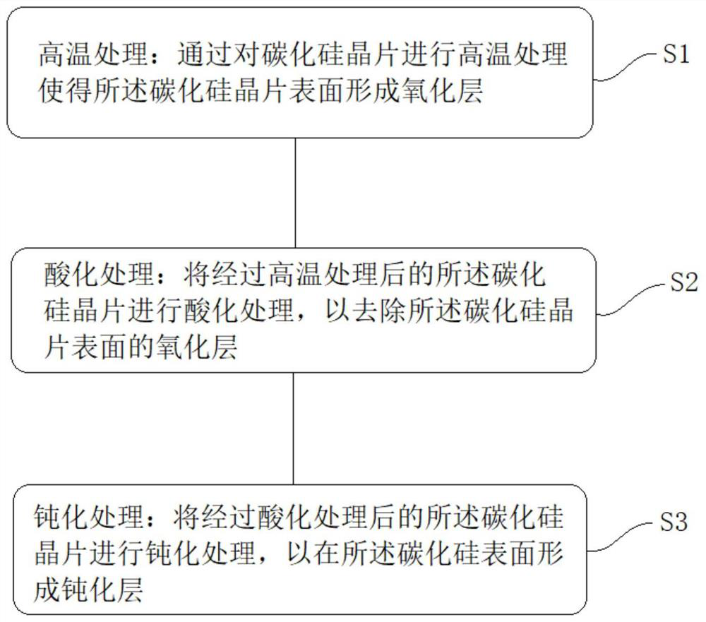
[0048] Put the silicon carbide wafer A that has undergone chemical mechanical polishing (CMP) into a holding furnace in a pure oxygen atmosphere (oxygen content ≥ 99%, pressure 1.2 times atmospheric pressure), and hold at a holding temperature of 800°C for 3 minutes.
[0049] Immerse the high-temperature-treated silicon carbide wafer A in a mixed solution of hydrofluoric acid and hydrochloric acid with a volume ratio of 1:15, and perform megasonic cleaning at room temperature with a megasonic frequency of 1000 kHz and a cleaning time of 2 minutes; Rinse both sides with Ou ultra-pure deionized water for 5 minutes. Wherein, the mass concentration of hydrofluoric acid is 40%, and the mass concentration of hydrochloric acid is 36%, both of which are industrial standard reagents.
[0050] The silicon carbide wafer A after pickling and rinsing was immersed in 18.25 megohm ultrapure deionized water at a temperature of 100°C for 15 minutes, and finally blown dry with nitrogen. Wherei...
Embodiment 2
[0052] Put the silicon carbide wafer B that has undergone chemical mechanical polishing (CMP) into a holding furnace in a pure oxygen atmosphere (oxygen content ≥ 99%, pressure 1.2 times atmospheric pressure), and hold at a holding temperature of 1000°C for 3 minutes.
[0053] Immerse the silicon carbide wafer B that has been heat-insulated in a mixed solution of hydrofluoric acid and hydrochloric acid with a volume ratio of 1:15, and perform megasonic cleaning at room temperature with a megasonic frequency of 1000 kHz and a cleaning time of 3 minutes; then use 18.25 M Rinse both sides with Ou ultra-pure deionized water for 5 minutes. Wherein, the mass concentration of hydrofluoric acid is 40%, and the mass concentration of hydrochloric acid is 36%, both of which are industrial standard reagents.
[0054] Soak the pickled and rinsed silicon carbide wafer B in 18.25 megohm ultrapure deionized water at 100°C for 10 minutes, and finally dry it with nitrogen. Wherein, nitrogen is...
Embodiment 3
[0056] Put the silicon carbide wafer C that has undergone chemical mechanical polishing (CMP) into a holding furnace in a pure oxygen atmosphere (oxygen content ≥ 99%, pressure 1.1 times atmospheric pressure), and hold at a holding temperature of 1000°C for 6 minutes.
[0057] Dip the heat-insulated silicon carbide wafer C into a mixed solution of hydrofluoric acid and hydrochloric acid with a volume ratio of 2:15, and perform ultrasonic cleaning at room temperature for 2 minutes; Rinse both sides with water for 15 minutes. Wherein, the mass concentration of hydrofluoric acid is 40%, and the mass concentration of hydrochloric acid is 36%, both of which are industrial standard reagents.
[0058] The silicon carbide wafer C after pickling and rinsing was immersed in 18.25 megohm ultrapure deionized water at 100° C. for 8 minutes, and finally blown dry with nitrogen. Wherein, nitrogen is high-purity nitrogen with a mass fraction of 99.999%, and the temperature is room temperatur...
PUM
 Abstract
Description
Claims
Application Information
 - Generate Ideas
- Intellectual Property
- Life Sciences
- Materials
- Tech Scout
- Unparalleled Data Quality
- Higher Quality Content
- 60% Fewer Hallucinations
Browse by: Latest US Patents, China's latest patents, Technical Efficacy Thesaurus, Application Domain, Technology Topic, Popular Technical Reports.
© 2025 PatSnap. All rights reserved.Legal|Privacy policy|Modern Slavery Act Transparency Statement|Sitemap|About US| Contact US: help@patsnap.com