


Quick Research
Generate reliable direction feasibility study reports for your R&D in just a few steps.

Technical Q&A
Discover and master advanced knowledge NOW. Basics, ideas, possibilities, all at once.

Find Solutions
As an expert in R&D theories, this can generate solutions to your technical problems instantly.

Evaluate Feasibility
Analyze your overall solution with one click, know your potential R&D risks in advance.

Monitor Landscape
Get weekly tech updates, stay abreast of the latest tech innovations and key insights.
Preparation of SiC MOSFET based on high-k gate dielectric and low-temperature ohmic contact process
A technology of ohmic contact and gate dielectric, applied in semiconductor/solid-state device manufacturing, electrical components, transistors, etc., can solve problems such as low mobility, achieve the effect of reducing carbon cluster density and improving channel mobility
- Summary
- Abstract
- Description
- Claims
- Application Information
AI Technical Summary
Problems solved by technology
Method used
Image

Examples
Embodiment 1
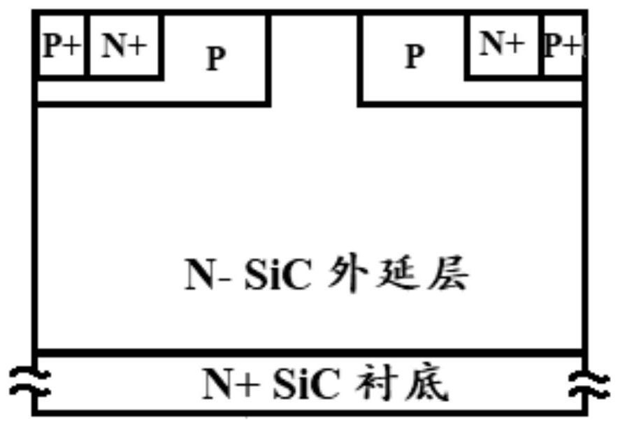
[0042] (1) The epitaxial N-type lightly doped SiC layer (thickness 13 μm, doping concentration 6×10 13 cm -3 ) SiC substrate cleaning; the cleaning process includes: standard RCA cleaning; high-temperature oxidation of silicon carbide epitaxial wafers to form a sacrificial oxide layer, and then corrode the sacrificial oxide layer until the surface oxide layer is completely removed.
[0043] (2) if figure 1 As shown, three kinds of implanted regions can be formed in the substrate. The three injection regions are respectively a P-type injection region, an N+ type injection region, and a P+ type injection region. Specifically, the N+ type implantation region is arranged between the P and P+ type implantation regions. P-type and P+-type implantation regions are formed by implanting aluminum and phosphorus ions. According to the embodiment, can inject 10 15 -10 18 cm -3 Doping concentration of P-type ions. Similarly, an N+ type implantation region is formed by implanting n...
Embodiment 2
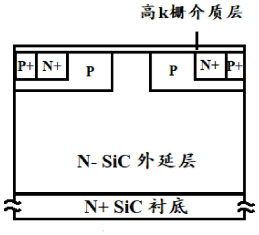
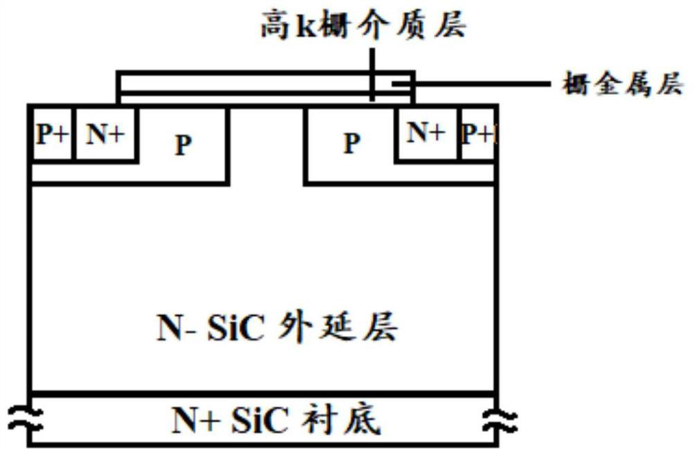
[0054] The high-k dielectric layer in step (3) in Example 1 can be replaced. In this example, the ALD method is used to grow La 2 o 5 (5nm) / Al 2 o 3 (45nm) medium layer, its thickness can be selected as 50nm. Other conditions do not change, and are all identical with embodiment 1.
[0055] Calculation process is identical with embodiment 1, for this laminated structure C ox =5.5×10 -11 F / m, other experimental data remain unchanged. In this embodiment, the interface state density can reach 7×10 11 -10 12 cm -2 eV -1 , with a mobility of 35cm 2 / Vs, the critical breakdown electric field strength can reach 8.7MV / cm.
Embodiment 3
[0057] The high-k dielectric layer in step (3) in Example 1 can be replaced. In this example, SiO grown by CVD method is selected. 2 (5nm) / AlN(45nm) dielectric layer, the thickness of which can be 50nm. Other conditions do not change, and are all identical with embodiment 1.
[0058] Calculation process is identical with embodiment 1, for this laminated structure C ox =6.2×10 -11 F / m, other experimental data remain unchanged. In this embodiment, the interface state density can reach 7×10 10 -4×10 12 cm -2 eV -1 , with a mobility of 26cm 2 / Vs, the critical breakdown electric field can reach 16.8MV / cm.
PUM
| Property | Measurement | Unit |
|---|---|---|
| Thickness | aaaaa | aaaaa |
| Doping concentration | aaaaa | aaaaa |
| Thickness | aaaaa | aaaaa |
Abstract
Description
Claims
Application Information
 - R&D Engineer
- R&D Manager
- IP Professional
- Industry Leading Data Capabilities
- Powerful AI technology
- Patent DNA Extraction
Browse by: Latest US Patents, China's latest patents, Technical Efficacy Thesaurus, Application Domain, Technology Topic, Popular Technical Reports.
© 2024 PatSnap. All rights reserved.Legal|Privacy policy|Modern Slavery Act Transparency Statement|Sitemap|About US| Contact US: help@patsnap.com