5G ceramic filter film material and preparation method thereof
A technology of ceramic filter and membrane layer, which is applied in metal material coating process, coating, ion implantation plating, etc., which can solve the problems of high relative processing cost of sintering, low bonding strength of metal and ceramic, and environmental pollution of electroless plating/electroplating and other problems, to achieve the effect of good deposition film quality, low bonding strength and compact structure
- Summary
- Abstract
- Description
- Claims
- Application Information
AI Technical Summary
Problems solved by technology
Method used
Image
Examples
Embodiment 1
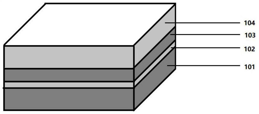
[0042] A preparation method for a 5G ceramic filter membrane material, specifically comprising the steps of:
[0043] S01: Carry out wet sandblasting, degreasing and degreasing treatment on the surface of the ceramic substrate; the particle size of the sand during wet blasting on the surface of the substrate is 300 mesh, and the wet spraying treatment time is 5s / piece; then the treated substrate is immersed in acetone, Ultrasonic cleaning with alcohol to remove oil and fat, and set aside;
[0044] S02: Using alloy metal NiCr as the cathode, use multi-arc targets to sputter and clean the cleaned ceramic substrate at the same time, where each target has an arc starting current of 100A, and the cleaning time is 30 minutes, and each group has three targets, a total of one group of alloy metal target to obtain an alloy layer with a deposition thickness of 0.1 μm;
[0045] S03: Using Cu as the cathode, a cylindrical multi-arc target is used to deposit a connecting layer with a thic...
Embodiment 2
[0048] A preparation method for a 5G ceramic filter membrane material, specifically comprising the steps of:
[0049] S01: Carry out wet sandblasting, degreasing and degreasing treatment on the surface of the ceramic substrate; the particle size of the sand during wet blasting on the surface of the substrate is 300 mesh, and the wet spraying treatment time is 5s / piece; then the treated substrate is immersed in acetone, Ultrasonic cleaning with alcohol to remove oil and fat, and set aside;
[0050] S02: Using alloy metal NiCu as the cathode, use multi-arc targets to sputter and clean the cleaned ceramic substrate at the same time, wherein each target has an arc starting current of 100A, and the cleaning time is 30 minutes, and each group has three targets, a total of one group of alloy metal target to obtain an alloy layer with a deposition thickness of 0.1 μm;
[0051] S03: Using Cu as the cathode, a cylindrical multi-arc target is used to deposit a connecting layer with a th...
PUM
| Property | Measurement | Unit |
|---|---|---|
| thickness | aaaaa | aaaaa |
| thickness | aaaaa | aaaaa |
| thickness | aaaaa | aaaaa |
Abstract
Description
Claims
Application Information
 - R&D
- Intellectual Property
- Life Sciences
- Materials
- Tech Scout
- Unparalleled Data Quality
- Higher Quality Content
- 60% Fewer Hallucinations
Browse by: Latest US Patents, China's latest patents, Technical Efficacy Thesaurus, Application Domain, Technology Topic, Popular Technical Reports.
© 2025 PatSnap. All rights reserved.Legal|Privacy policy|Modern Slavery Act Transparency Statement|Sitemap|About US| Contact US: help@patsnap.com


