
Semiconductor device manufacturing method

一种制造方法、半导体的技术,应用在半导体/固态器件制造、半导体器件、半导体/固态器件零部件等方向,能够解决定位部件倾斜配置等问题,达到抑制品质降低、可靠接合的效果

Pending Publication Date: 2020-08-25
FUJI ELECTRIC CO LTD
View PDF2 Cites 0 Cited by
  • Summary
  • Abstract
  • Description
  • Claims
  • Application Information

AI Technical Summary

Problems solved by technology

However, it is not described that since the positioning member moves along the main body, a plurality of positioning members may be arranged obliquely in the frame.

Method used


Image

  • Semiconductor device manufacturing method
  • Semiconductor device manufacturing method
  • Semiconductor device manufacturing method

Examples


no. 1 Embodiment approach

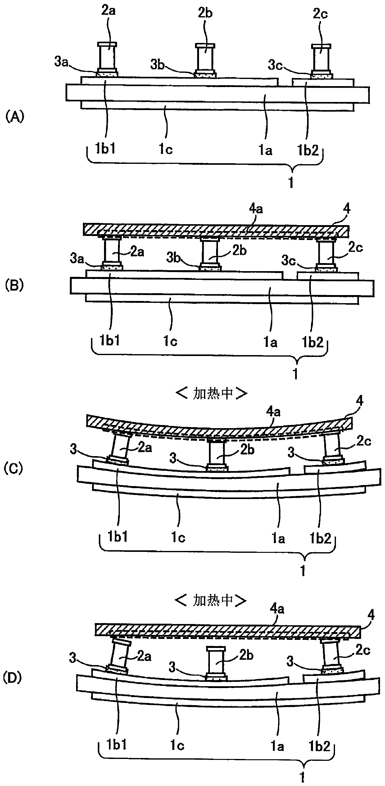
[0067] Below, with reference to the accompanying drawings, use figure 1 A method of manufacturing the semiconductor device according to the first embodiment will be described. figure 1 It is a figure for demonstrating each process of the manufacturing method of the semiconductor device of 1st Embodiment. It should be stated that in figure 1 (A)~ figure 1 (C) is a side view showing, in time series, the steps related to the reflow soldering step in the manufacturing method of the semiconductor device. in addition, figure 1 (D) shows for figure 1 Reference example of the process of (C).

[0068] First, a multilayer substrate 1 and a plurality of contact members 2a to 2c are prepared. The laminated substrate 1 has an insulating layer 1a, circuit pattern layers 1b1 and 1b2 formed on the front surface of the insulating layer 1a, and a metal layer 1c formed on the back surface of the insulating layer 1a and having a larger area than the circuit pattern layers 1b1 and 1b2. In suc...

no. 2 Embodiment approach

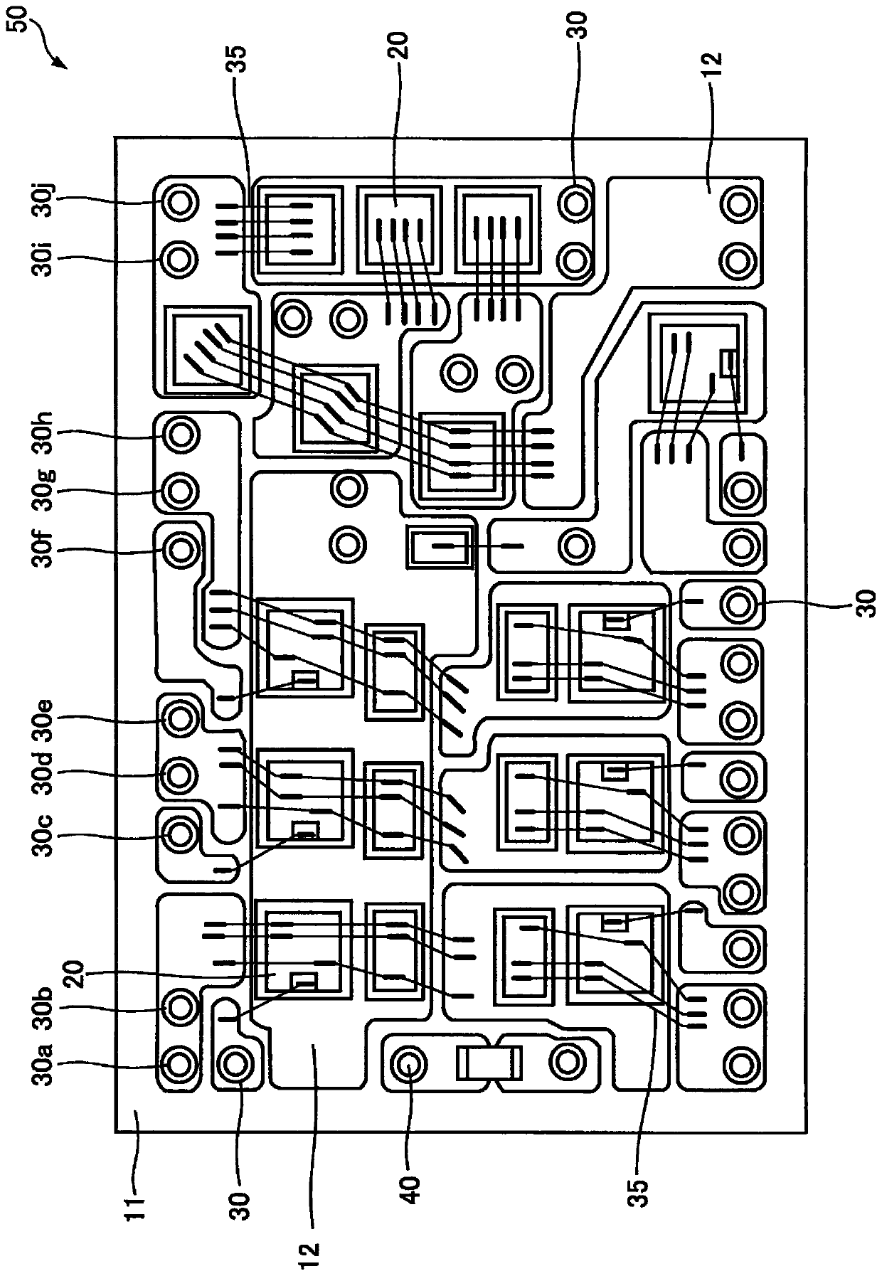
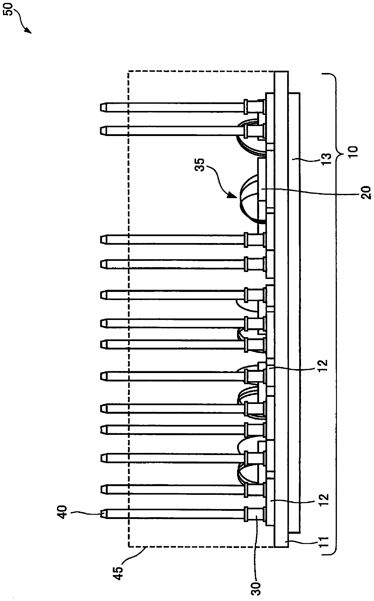
[0075] In the second embodiment, the method of manufacturing the semiconductor device according to the first embodiment will be described more specifically. First, use figure 2 with image 3 A semiconductor device will be described. figure 2 It is a plan view showing the semiconductor device of the second embodiment, image 3 It is a side view showing the semiconductor device of the second embodiment. should be explained, figure 2 Illustration of packaged components is omitted. exist image 3 In , packaged components are indicated by dotted lines. In addition, in the second embodiment, the plurality of circuit pattern layers 12, the plurality of semiconductor elements 20, the plurality of contact members 30, the plurality of bonding wires 35, and the plurality of external connection terminals 40 are not distinguished, and the same symbols are attached. and are described with the same symbols. In addition, about the structure other than these structures, a plurality ...


PUM

PropertyMeasurementUnit
diameteraaaaaaaaaa
diameteraaaaaaaaaa

Abstract

The invention provides a method of manufacturing a semiconductor device. A contact member can be reliably joined. A pressing region (4a) set on the main surface of a flat-plate-shaped pressing tool (4) is disposed on contact members (2a-2c). Then, while heating, the pressing region (4a) of the pressing tool (4) is tilted in accordance with warpage occurring in a laminated substrate (1), and the contact members (2a-2c) are pressed toward the laminated substrate (1). As a result, when pressing is performed for bonding the contact members (2a-2c), the contact members (2a-2c) can be reliably pressed against the laminated substrate (1) even if warpage occurs in the laminated substrate (1) due to heating and the positions of the contact members (2a-2c) are shifted.

Description

technical field [0001] The present invention relates to a method of manufacturing a semiconductor device. Background technique [0002] Semiconductor devices including semiconductor elements such as IGBT (Insulated Gate Bipolar Transistor: Insulated Gate Bipolar Transistor) and power MOSFET (Metal Oxide Semiconductor Field Effect Transistor: Metal Oxide Semiconductor Field Effect Transistor) are used as power conversion devices, for example. Such a semiconductor device includes a ceramic circuit board having an insulating layer, and a plurality of circuit pattern layers formed on the front surface of the insulating layer and on which semiconductor elements are disposed. In addition, a cylindrical contact member for mounting an external connection terminal is provided on a predetermined region of the circuit pattern layer via solder. [0003] When manufacturing such a semiconductor device, first, a contact member is arranged via solder on a predetermined region of a circuit ...

Claims


Application Information

Patent Timeline
Patent Type & Authority Applications(China)
IPC IPC(8): H01L25/16H01L25/07H01L25/00
CPCH01L25/16H01L25/072H01L25/50H01L2224/73265B23K1/0016B23K3/087B23K2101/40H01L23/49811H01L23/3735H01L21/4853H01L23/5386H05K1/0306H05K3/341H05K3/3494H05K2203/0278H05K3/4015H05K2203/1509H05K2201/10242H05K2201/1031H05K2201/0367H05K2203/068H01L2224/48139H01L2224/48227H01L2224/49111H01L2224/0603H01L2224/45144H01L2224/45139H01L2224/45147H01L2224/45124H01L2224/45015H01L24/45H01L24/48H01L24/49H01L24/06H01L2924/19105H01L2224/83192H01L2224/29101H01L2224/83801H01L2224/92247H01L24/73H01L24/92H01L24/29H01L24/32H01L24/83Y02P70/50H01L2224/48096H01L2924/00014H01L2924/2076H01L2924/014H01L2224/32225H01L2924/00012H01L2224/32245H01L2224/48247H01L2924/00H05K3/301H05K3/303H01L2224/48091B23K3/04
Inventor 万·阿札·宾·万·马特横山岳
Owner FUJI ELECTRIC CO LTD
Learn More