Photoetching method

A photolithography and photoresist technology, applied in the field of photolithography, can solve problems such as tearing of metal layers

Active Publication Date: 2020-07-10
ORIGIN QUANTUM COMPUTING TECH (HEFEI) CO LTD
View PDF4 Cites 6 Cited by
  • Summary
  • Abstract
  • Description
  • Claims
  • Application Information

AI Technical Summary

Problems solved by technology

[0004] Aiming at the problem that the metal layer in the deposition area is likely to be torn in the process of peeling off the adhesive in the related photolithography technology, the present invention provides a photolithography method ,it includes:

Method used


Image

  • Photoetching method
  • Photoetching method
  • Photoetching method

Examples


Embodiment Construction

[0042] Embodiments of the present invention will be described below in conjunction with specific examples and accompanying drawings, and those skilled in the art can easily understand other advantages and effects of the present invention from the content disclosed in this specification. The present invention can also be implemented or applied through other different specific implementation modes, and various modifications or changes can be made to the details in this specification based on different viewpoints and applications without departing from the spirit of the present invention.

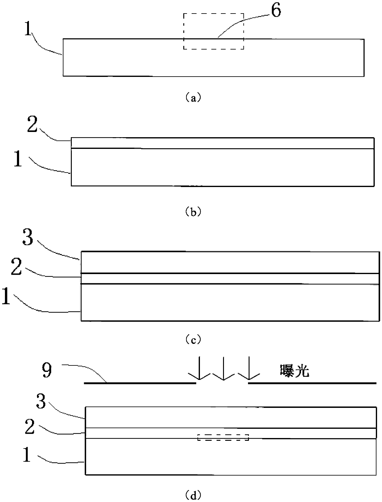
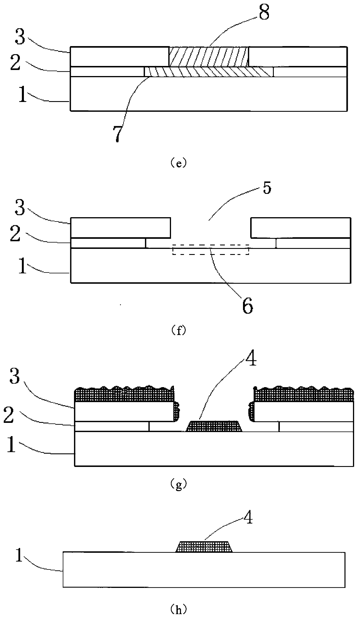
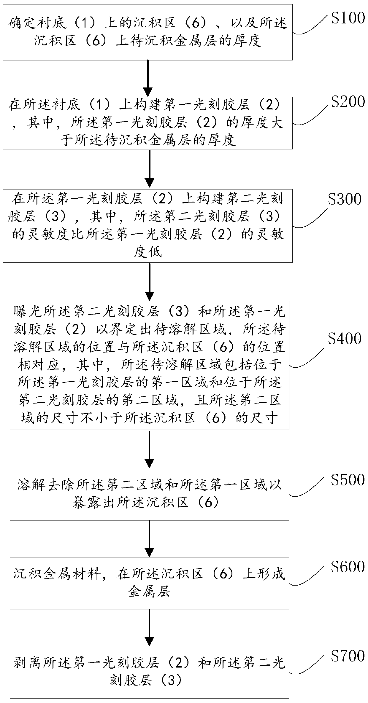
[0043] combine figure 2 , a photolithography method, comprising step S100 to step S700, wherein:

[0044] Step S100, such as figure 1 As shown in (a), the deposition area 6 on the substrate 1 and the thickness of the metal layer to be deposited on the deposition area 6 are determined. In this embodiment, an aluminum layer with a thickness of 80 nm is to be deposited. Wherein, the substrate ...


PUM

PropertyMeasurementUnit
thicknessaaaaaaaaaa
thicknessaaaaaaaaaa

Abstract

The invention discloses a photoetching method, and belongs to the field of integrated circuit manufacturing. The method comprises the following steps of: coating photoresist with higher sensitivity ona substrate with a determined deposition area to form a first photoresist layer, and the photoresist being thicker than a metal layer to be deposited; coating photoresist with lower sensitivity to form a second photoresist layer; defining a to-be-dissolved area corresponding to the deposition area in position through one-time exposure, and the to-be-dissolved area comprising a first area positioned in the first photoresist layer and a second area positioned in the second photoresist layer; dissolving and removing the photoresist in the first area and the second area by using a developing solution and the like so as to expose a deposition area; and depositing a metal material after the first photoresist layer and the second photoresist layer are deposited so that no adhesion phenomenon occurs between metal material residues on the surfaces and the side walls of the metal layer and the second photoresist layer formed in the deposition area. Therefore, when the first photoresist layer and the second photoresist layer are peeled off after the metal material is deposited, the metal layer in the deposition area cannot be torn off.

Description

technical field [0001] The invention belongs to the field of integrated circuit manufacturing, and more specifically relates to a photolithography method. Background technique [0002] With the continuous development of integrated circuit technology, the integration level of IC devices has been continuously improved, and the feature size has become smaller and smaller. Therefore, the requirements for the manufacturing process of integrated circuits are becoming more and more stringent, and slight process deviations will lead to changes in device performance, which in turn will cause the overall circuit to deviate from the design requirements. [0003] Among them, the photolithography process mainly includes the steps of gluing-pre-baking-exposure-developing-film-hardening-etching-removing, etc. It mainly uses the photochemical reaction of the photosensitive resist coating, combined with the corrosion method on various thin films or The desired pattern is prepared on the sil...

Claims


Application Information

Patent Timeline
Patent Type & Authority Applications(China)
IPC IPC(8): G03F7/00C23C14/30C23C14/14C23C14/04
CPCG03F7/0035C23C14/30C23C14/14C23C14/042
Inventor 赵勇杰
Owner ORIGIN QUANTUM COMPUTING TECH (HEFEI) CO LTD
Why Eureka
Try Eureka