Silicon nitride gap filling layer and method for forming same

A filling layer and silicon nitride technology, which is applied in electrical components, semiconductor/solid-state device manufacturing, circuits, etc., can solve the problems of contact window etching residue, insufficient trench filling ability, and easy gap generation, so as to increase ion gain and improve Gully filling ability, the effect of avoiding the formation of gaps

Active Publication Date: 2010-06-02
UNITED MICROELECTRONICS CORP
View PDF4 Cites 0 Cited by
  • Summary
  • Abstract
  • Description
  • Claims
  • Application Information

AI Technical Summary

Problems solved by technology

[0007] For increasing the thickness of the contact etch stop layer, please refer to figure 1 , due to the insufficient gap-fill (Gap-Fill) ability of the excessively thick silicon nitride layer 102 and the subsequently deposited dielectric layer 104, it is easy to generate gaps (seam) or holes (void) 100, such as figure 1 As shown, therefore, it will cause the problem of subsequent contact etching residue, or cause the short circuit problem between the contact window and the contact window or between the contact window and the gate.
On the other hand, if the aging process is performed after the deposition process in order to further increase the stress of the thick silicon nitride layer, the problem of tearing of the silicon nitride layer will be caused due to the excessive thickness.

Method used


Image

  • Silicon nitride gap filling layer and method for forming same
  • Silicon nitride gap filling layer and method for forming same
  • Silicon nitride gap filling layer and method for forming same

Examples


Embodiment Construction

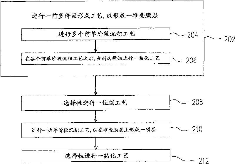
[0055] figure 2 It is a flow chart of a method for forming a silicon nitride gap-fill layer according to an embodiment of the present invention.

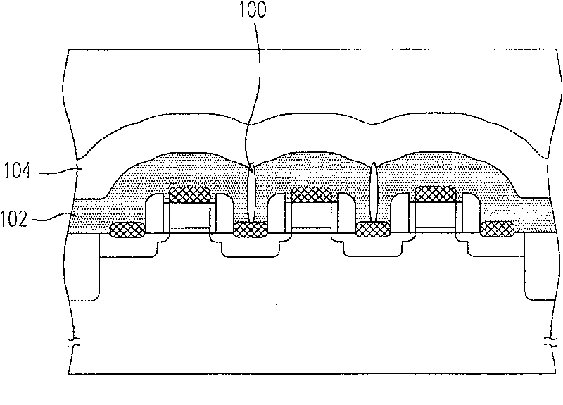
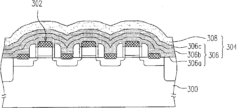
[0056] Please refer to figure 2 , the method for forming a silicon nitride gap-fill layer in this embodiment is to first perform a multi-stage formation process to form a stacked film layer, step 202 . Then, a subsequent single-stage deposition process is performed to form a top layer on the stacked film layers, step 210 . In step 210, the thickness of the top layer formed by the subsequent single-stage deposition process is greater than the thickness of each film layer of the stacked film layer formed by the previous multi-stage formation process in step 202, so that the stacked film layer forms a dense film; and the top layer is Constitute a loose film (sparse film).

[0057] Step 202, the pre-multi-stage formation process, including performing multiple pre-single-stage deposition processes, step 204, and after each pre-singl...


PUM

PropertyMeasurementUnit
thicknessaaaaaaaaaa
thicknessaaaaaaaaaa

Abstract

The invention relates to a method for forming a packing layer in the clearance of silicon nitride, and the method comprises the following steps: firstly, a former multistage forming process is carriedout to form a stacking film layer on a substrate, thus forming a dense film, and then, a later single stage deposition process is carried out to form a top layer on the stacking film layer, thus forming a loose film, wherein, the thickness of the top layer accounts for more than 10 percent of the total thickness of the packing layer in the clearance of silicon nitride.

Description

technical field [0001] The present invention relates to a semiconductor gap filling layer and its forming method, and in particular to a silicon nitride gap filling layer and its forming method. Background technique [0002] With the development of electronic equipment such as communication technology, the operation speed of transistors is getting faster and faster. However, due to the limitation of the moving speed of electrons and holes in the silicon channel, the application range of the transistor is also limited. [0003] Using the control of mechanical-stress in the channel to change the moving speed of electrons and holes in the channel is a method that can overcome the limitation caused by the shrinkage of the device. [0004] It is known that a method of using silicon nitride as a contact etching stop layer (contact etching stop layer, CESL) to generate strain (Strain) to affect the driving current and ion gain (IonGain) of the transistor to improve the performance...

Claims


Application Information

Patent Timeline
Patent Type & Authority Patents(China)
IPC IPC(8): H01L21/02
Inventor 陈能国谢朝景黄建中
Owner UNITED MICROELECTRONICS CORP
Why Eureka
Try Eureka