A processing method of monocrystalline silicon wafer, monocrystalline silicon wafer and solar cell
A processing method and technology of monocrystalline silicon wafers, which are applied in the field of solar cells, can solve the problems of low conversion effect, and achieve the effects of increasing the specific surface area per unit of the upper surface, good absorption efficiency, and uniform p-n junction
- Summary
- Abstract
- Description
- Claims
- Application Information
AI Technical Summary
Problems solved by technology
Method used
Image
Examples
preparation example Construction
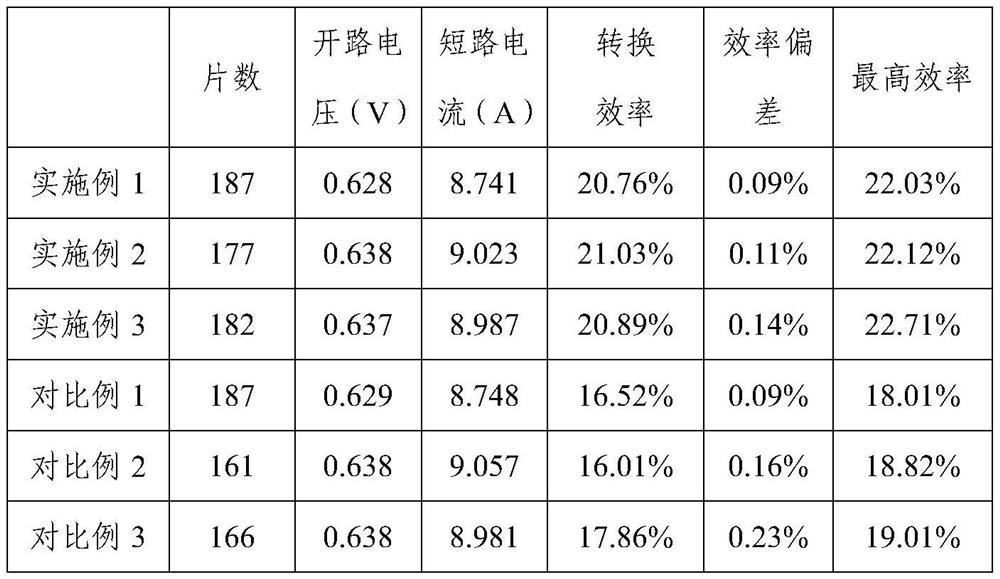
[0051] This embodiment relates to a method for preparing a monocrystalline silicon solar cell, and the processing of a monocrystalline silicon wafer includes the following steps:
[0052]1) Alkali polishing, the cut monocrystalline silicon wafer is polished with a sodium hydroxide solution with a concentration of 4wt%, the polishing temperature is controlled at 60°C, and the polishing time is controlled at 160s to remove the damaged layer of the silicon wafer;
[0053] 2) Pure iron sputtering etching. Firstly, the alkali-polished silicon wafer was washed with deionized water and then dried. Then, it was installed on the target frame as a target material. The pure iron powder sample dish with an average particle size of 60 μm was sputtered. The radiation power is 300W, and the sputtering time is 60min; then, the iron-containing silicon wafer is cleaned with a mixed acid with a hydrochloric acid concentration of 15wt% and a nitric acid concentration of 5wt%, and then cleaned with...
Embodiment 2
[0060] This embodiment relates to a method for preparing a monocrystalline silicon solar cell, and the processing of a monocrystalline silicon wafer includes the following steps:
[0061] 1) Alkali polishing, the cut monocrystalline silicon wafer is polished with a sodium hydroxide solution with a concentration of 2wt%, the polishing temperature is controlled at 60°C, and the polishing time is controlled at 150s to remove the damaged layer of the silicon wafer;
[0062] 2) Pure iron sputtering etching. Firstly, the alkali-polished silicon wafer was washed with deionized water and then dried. Then it was installed on the target frame as a target. The pure iron powder sample dish with an average particle size of 50 μm was sputtered The radiation power is 50W, and the sputtering time is 30min; then, the iron-containing silicon wafer is cleaned with a mixed acid with a hydrochloric acid concentration of 12wt% and a nitric acid concentration of 3wt%, and then cleaned with deionized ...
Embodiment 3
[0070] This embodiment relates to a method for preparing a monocrystalline silicon solar cell, comprising the following steps:
[0071] 1) Alkali polishing, the cut monocrystalline silicon wafer is polished with a sodium hydroxide solution with a concentration of 4wt%, the polishing temperature is controlled at 60°C, and the polishing time is controlled at 160s to remove the damaged layer of the silicon wafer;
[0072] 2) Pure iron sputtering etching. Firstly, the alkali-polished silicon wafer was washed with deionized water and then dried. Then, it was installed on the target frame as a target material. The pure iron powder sample dish with an average particle size of 60 μm was sputtered. The radiation power is 300W, and the sputtering time is 60min; then, the iron-containing silicon wafer is cleaned with a mixed acid with a hydrochloric acid concentration of 15wt% and a nitric acid concentration of 5wt%, and then cleaned with deionized water to remove iron and silicon powder....
PUM
| Property | Measurement | Unit |
|---|---|---|
| thickness | aaaaa | aaaaa |
| particle size | aaaaa | aaaaa |
Abstract
Description
Claims
Application Information
 - R&D
- Intellectual Property
- Life Sciences
- Materials
- Tech Scout
- Unparalleled Data Quality
- Higher Quality Content
- 60% Fewer Hallucinations
Browse by: Latest US Patents, China's latest patents, Technical Efficacy Thesaurus, Application Domain, Technology Topic, Popular Technical Reports.
© 2025 PatSnap. All rights reserved.Legal|Privacy policy|Modern Slavery Act Transparency Statement|Sitemap|About US| Contact US: help@patsnap.com

