High temperature resistant flexible array antenna and manufacturing method thereof
An array antenna, high-temperature flexible technology, applied in antennas, antenna arrays, and devices for manufacturing antenna arrays, etc., can solve problems such as unsuitable antenna development needs, weak ability to receive signals in multiple directions, and limited directivity of a single antenna. To achieve the effect of broadening the diversity of radiation and reception, being flexible and reducing the volume
- Summary
- Abstract
- Description
- Claims
- Application Information
AI Technical Summary
Problems solved by technology
Method used
Image
Examples
Embodiment 1
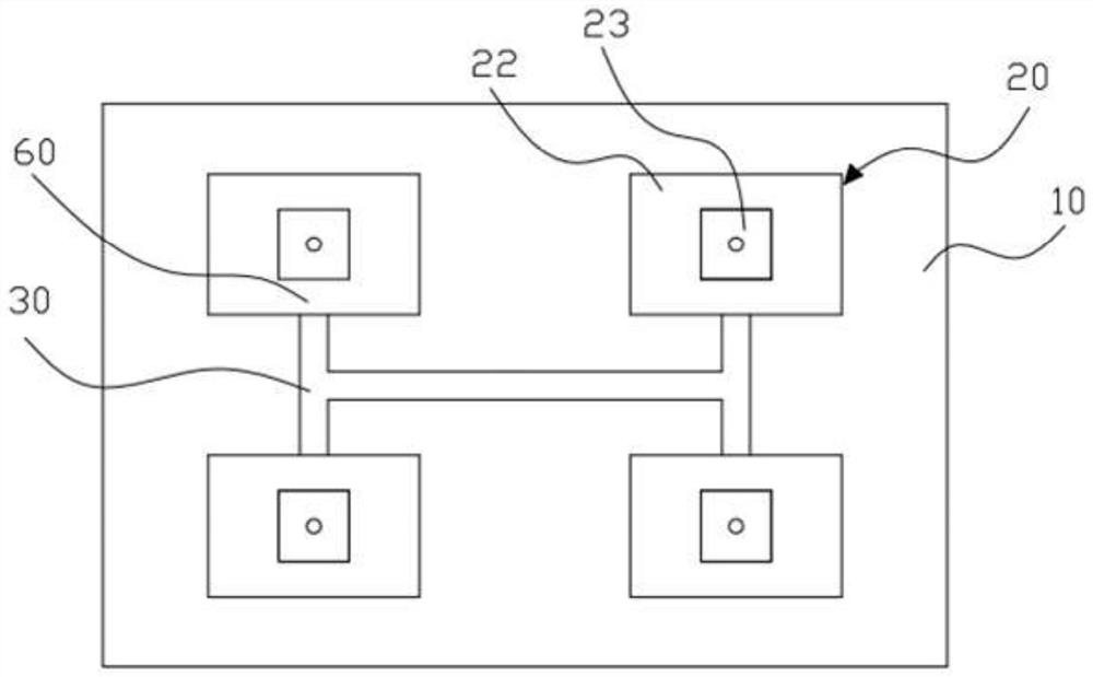
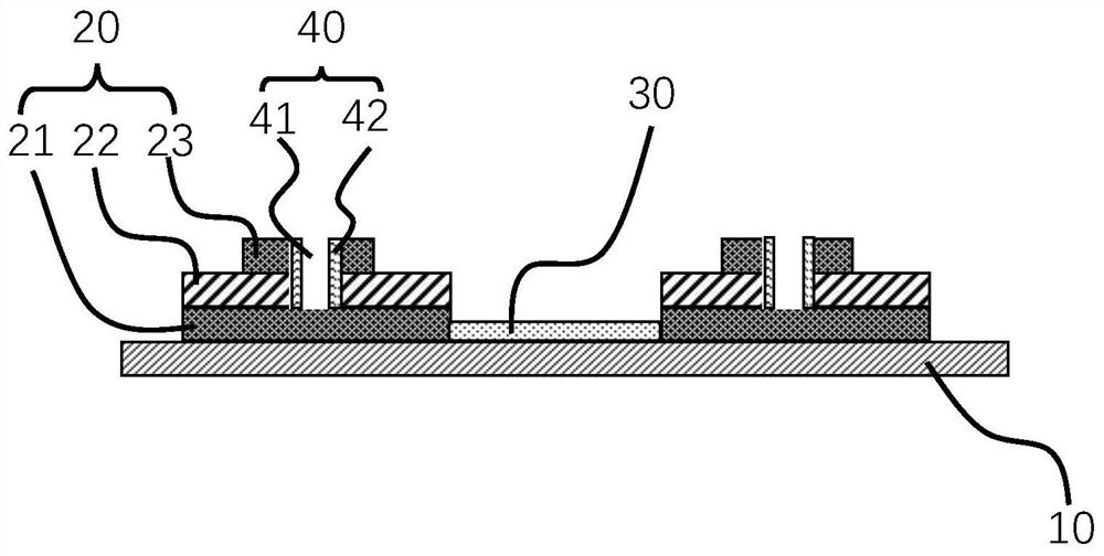
[0086] A circular alumina-based ceramic material substrate 22 with a thickness of 0.1 mm and a diameter of 10 mm is drilled through a hole 41, placed in a beaker with absolute ethanol, cleaned for 5 minutes in an ultrasonic wave with a power of 40 W, and the substrate 22 is taken out. And dry at 100° C., and form a high-temperature silver paste layer on the substrate 22 by using a screen printing process. The patterned screen during screen printing has a mesh of 200 meshes and a squeegee angle of 30°. After the silk screen printing is completed, the silver paste layer is dried to form the metal layer 23 , and the hole metal layer 42 is formed by stuffing the metal paste into the through hole 41 and drying.
[0087] Place a flexible mica sheet 10 with a thickness of 10 μm in a vacuum chamber and evacuate to 3×10 -3 Pa. Fill the vacuum chamber with Ar so that the vacuum degree is 0.1Pa, turn on the power supply of the heater, heat the flexible mica sheet 10 to 50°C, turn on the...
Embodiment 2
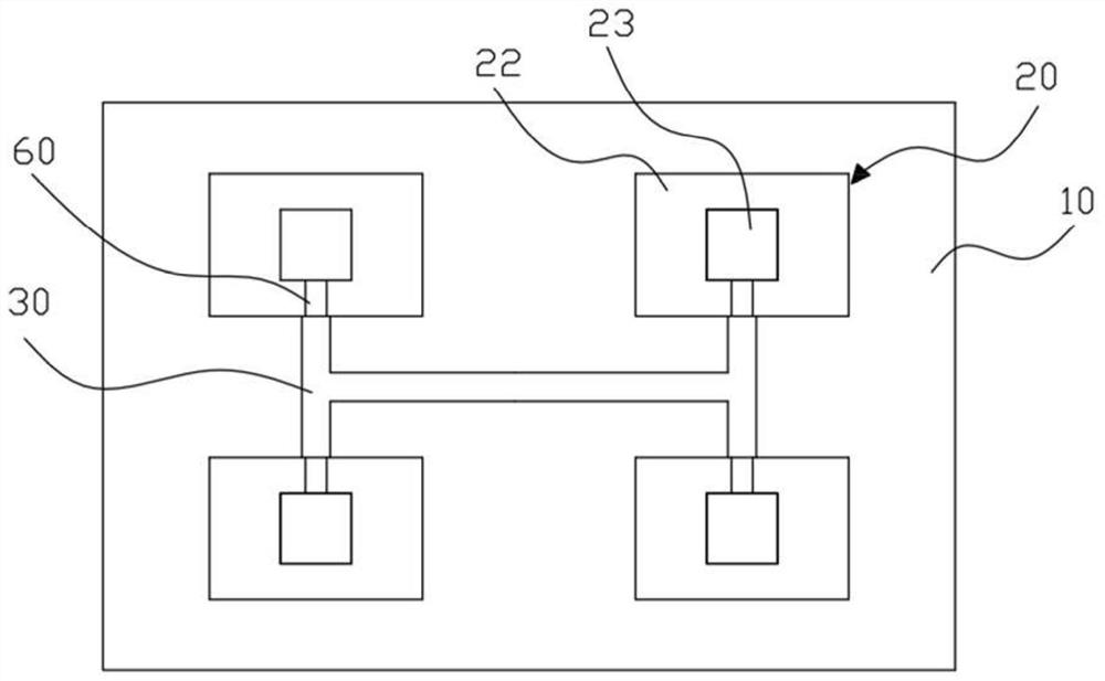
[0090] Place a square magnesium titanate-based ceramic substrate 22 with a thickness of 2mm and a side length of 10mm in a beaker filled with absolute ethanol, clean it in an ultrasonic wave with a power of 40W for 30min, take out the substrate 22 and bake it at 100°C Drying, using 3D printing to form a high-temperature platinum paste on the surface and side walls of the substrate 22 , and drying the platinum paste layer to form the metal layer 23 and the side wall metal layer 60 .
[0091] Place a flexible mica sheet 10 with a thickness of 50 μm in a vacuum chamber and evacuate to 3×10 -3 Pa. Fill the vacuum chamber with O 2 , so that the vacuum degree is 0.5 Pa, turn on the power supply of the heater, heat the flexible mica sheet 10 to 150°C, turn on the Plasma power supply, adjust the voltage to 2000V, and process the flexible mica sheet 10 for 20 minutes through the generated Ar plasma. When the flexible mica sheet 10 is cooled to room temperature in an argon atmosphere,...
Embodiment 3
[0094] Place the mask plate on a circular alumina ceramic substrate 22 with a thickness of 1 mm and a diameter of 10 mm. The entire assembly is placed in a vacuum chamber and evacuated to 3×10 -3 Pa. Fill the vacuum chamber with Ar so that the degree of vacuum is 0.1Pa, turn on the magnetron sputtering power supply, adjust the current to 1A, and carry out magnetron sputtering deposition on the ceramic substrate 22 with the mask plate to lay the underlying metal Ti, and deposit The time is 30 s, the thickness is 10 nm, and then the thickened layer of metal Ag is deposited, the deposition time is 30 min, and the thickness is 2 μm, forming the metal layer 23 and the sidewall metal layer 60 .
[0095] Place a flexible mica sheet 10 with a thickness of 50 μm in a vacuum chamber and evacuate to 3×10 -3 Pa. Fill the vacuum chamber with O 2 , so that the vacuum degree is 0.5Pa, turn on the power supply of the heater, heat the flexible mica sheet 10 to 150°C, turn on the Plasma powe...
PUM
 Abstract
Description
Claims
Application Information
 - R&D
- Intellectual Property
- Life Sciences
- Materials
- Tech Scout
- Unparalleled Data Quality
- Higher Quality Content
- 60% Fewer Hallucinations
Browse by: Latest US Patents, China's latest patents, Technical Efficacy Thesaurus, Application Domain, Technology Topic, Popular Technical Reports.
© 2025 PatSnap. All rights reserved.Legal|Privacy policy|Modern Slavery Act Transparency Statement|Sitemap|About US| Contact US: help@patsnap.com


