Semiconductor structure and preparation method thereof

A semiconductor and manufacturing method technology, applied in the field of semiconductor structure and preparation, can solve the problems of poor isolation effect of shallow trench isolation structure, etc., achieve the effect of improving isolation effect, reducing narrow channel effect, and avoiding edge notch defects

Pending Publication Date: 2020-04-07
CHANGXIN MEMORY TECH INC
View PDF0 Cites 4 Cited by
  • Summary
  • Abstract
  • Description
  • Claims
  • Application Information

AI Technical Summary

Problems solved by technology

[0004] In view of the shortcomings of the prior art described above, the purpose of the present invention is to provide a semiconductor structure and a preparation method for solving the problem of poor isolation effect of the shallow trench isolation structure in the prior art

Method used


Image

  • Semiconductor structure and preparation method thereof
  • Semiconductor structure and preparation method thereof
  • Semiconductor structure and preparation method thereof

Examples


Embodiment 1

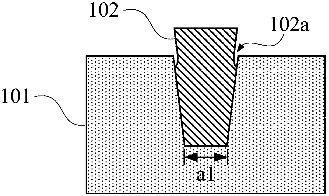
[0079] like figure 1 As shown, it is a schematic cross-sectional view of a shallow trench isolation structure obtained by using the prior art. The silicon dioxide dielectric layer 102 is filled in the trench formed on the silicon substrate 101 to form a shallow trench isolation structure, and in the subsequent process, it is generally necessary to use wet etching to remove the surface of the silicon substrate 101. The dielectric layer is simultaneously etched into the silicon dioxide dielectric layer 102 in the trench, and an edge gap 102a is formed at the edge of the trench. The edge notch 102a will form an additional leakage current channel in the subsequent process, which will affect the isolation effect and even cause the device to fail. In addition, the bottom width a1 of the shallow trench isolation structure also has a great influence on the leakage performance of the shallow trench isolation structure, and the narrow bottom width a1 will cause substrate leakage curren...

Embodiment 2

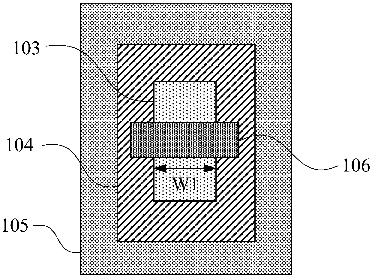
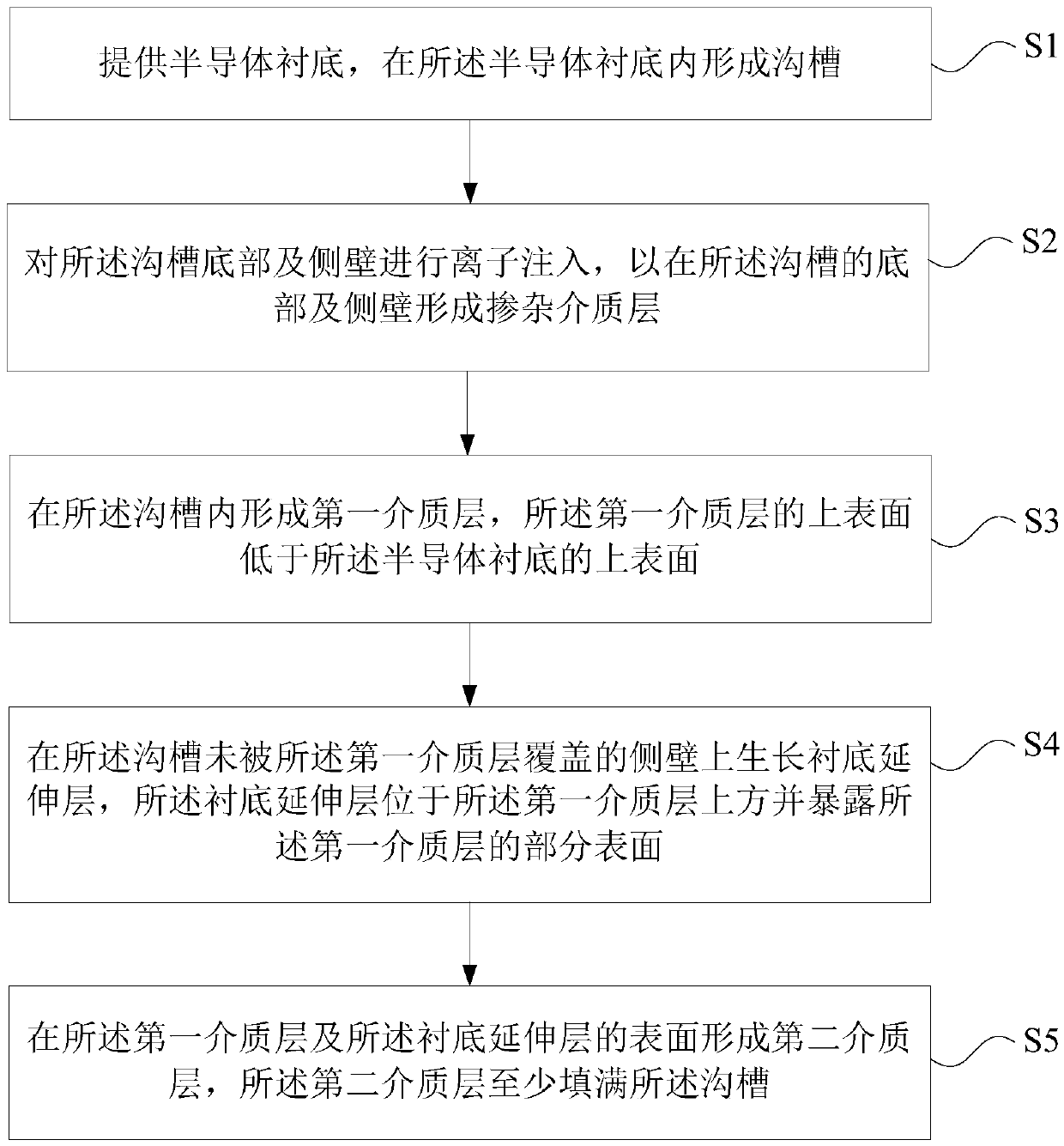
[0095] see Figure 14 , the present invention also provides a semiconductor structure, comprising:

[0096] semiconductor substrate 201;

[0097] a trench 201a is formed in the semiconductor substrate 201;

[0098] A doped dielectric layer 202 is formed on the bottom and sidewalls of the trench 201a;

[0099] The first dielectric layer 203 is formed in the trench 201a, and the upper surface of the first dielectric layer 203 is lower than the upper surface of the semiconductor substrate 201;

[0100] a substrate extension layer 201b, formed on the sidewall of the trench 201a not covered by the first dielectric layer 203, and extending to cover part of the surface of the first dielectric layer 203; and

[0101] The second dielectric layer 204 is formed on the surfaces of the first dielectric layer 203 and the substrate extension layer 201b, and at least fills the trench 201a.

[0102] like Figure 14 As shown, trenches 201a are formed in a semiconductor substrate 201, which...


PUM


Abstract

The invention provides a semiconductor structure and a preparation method thereof, and the preparation method comprises the following steps: 1), providing a semiconductor substrate, and forming a trench in the semiconductor substrate; 2) performing ion implantation on the bottom and the side wall of the trench to form a doped dielectric layer; 3) forming a first dielectric layer in the trench, wherein the upper surface of the first dielectric layer is lower than the upper surface of the semiconductor substrate; 4) growing a substrate extension layer located above the first dielectric layer onthe side wall, which is not covered by the first dielectric layer, of the trench, and exposing a part of the surface of the first dielectric layer; and 5) forming a second dielectric layer at least filling the trench on the surfaces of the first dielectric layer and the substrate extension layer. According to the shallow trench isolation structure, the substrate extension layer is formed to coverthe side wall of the dielectric layer at the edge of the protection trench, so that the formation of an edge gap defect is avoided, the area of an active region is increased, and the narrow channel effect is reduced; a shallow trench isolation structure with a wide trench bottom is obtained through ion implantation, the isolation effect is improved, and the product yield is improved.

Description

technical field [0001] The invention relates to the field of semiconductor integrated circuit manufacturing, in particular to a semiconductor structure and a preparation method. Background technique [0002] At present, Shallow Trench Isolation (STI) is widely used in the isolation process of 0.25um and below semiconductor technology nodes. Among them, the defects or parameters affecting the performance of the shallow trench isolation structure mainly include edge notch (divot) and the bottom width of the shallow trench isolation structure. In the prior art, the edge of the shallow trench isolation structure is often corroded in the subsequent wet etching to form edge notch defects, thereby causing device failure; in addition, as the device size decreases, the shallow trench isolation structure The bottom width of the transistor and the channel width of the transistor are also reduced, which also seriously affects the electrical performance of the device. [0003] Therefor...

Claims


Application Information

Patent Timeline
Patent Type & Authority Applications(China)
IPC IPC(8): H01L21/762
CPCH01L21/76224H01L21/76237
Inventor 刘梅花
Owner CHANGXIN MEMORY TECH INC
Why Eureka
Try Eureka