
N-type crystalline silicon PERT double-sided battery with new structure and preparation method of n-type crystalline silicon PERT double-sided battery

A double-sided battery and new structure technology, applied in the direction of circuits, photovoltaic power generation, electrical components, etc., can solve the problems of insufficient passivation, high cost, and low efficiency of the carrier metal electrode area, and achieve superior compactness and open circuit Effect of voltage and conversion efficiency improvement

Inactive Publication Date: 2020-03-13
SHANGHAI JIAO TONG UNIV
View PDF5 Cites 12 Cited by
  • Summary
  • Abstract
  • Description
  • Claims
  • Application Information

AI Technical Summary

Problems solved by technology

[0004] In view of the above-mentioned defects of the prior art, the technical problem to be solved by the present invention is to solve the problem of carrier recombination at the metal / semiconductor interface and the passivation of the metal electrode region is not superior enough, and the traditional method has higher cost and lower efficiency question

Method used


Image

  • N-type crystalline silicon PERT double-sided battery with new structure and preparation method of n-type crystalline silicon PERT double-sided battery
  • N-type crystalline silicon PERT double-sided battery with new structure and preparation method of n-type crystalline silicon PERT double-sided battery
  • N-type crystalline silicon PERT double-sided battery with new structure and preparation method of n-type crystalline silicon PERT double-sided battery

Examples


Embodiment 1

[0037] Embodiment 1: The preparation method of the new structure N-type crystalline silicon PERT bifacial battery of the present invention is as follows:

[0038] Step 1, prepare an n-type Cz single crystal silicon wafer with an industrial-grade crystal orientation of (100) as an n-type crystalline silicon substrate, and use sodium hydroxide solution to remove the damaged layer formed on the surface of the n-type crystalline silicon substrate due to wire cutting ;

[0039] Step 2, texture the n-type crystalline silicon substrate obtained in step 1 with an alkaline solution, and then perform standard RCA cleaning to obtain a pretreated silicon wafer;

[0040] Step 3, put the silicon wafers obtained in step 2 back to back into a traditional high-temperature diffusion furnace for BBr 3 Diffusion, forming p on the positive surface + emission level layer;

[0041] Step 4, using a nanosecond pulsed laser with a wavelength of 532 nm and a pulse energy between 80 μJ and 300 μJ to t...


PUM

PropertyMeasurementUnit
Thicknessaaaaaaaaaa
Resistivityaaaaaaaaaa
Thicknessaaaaaaaaaa

Abstract

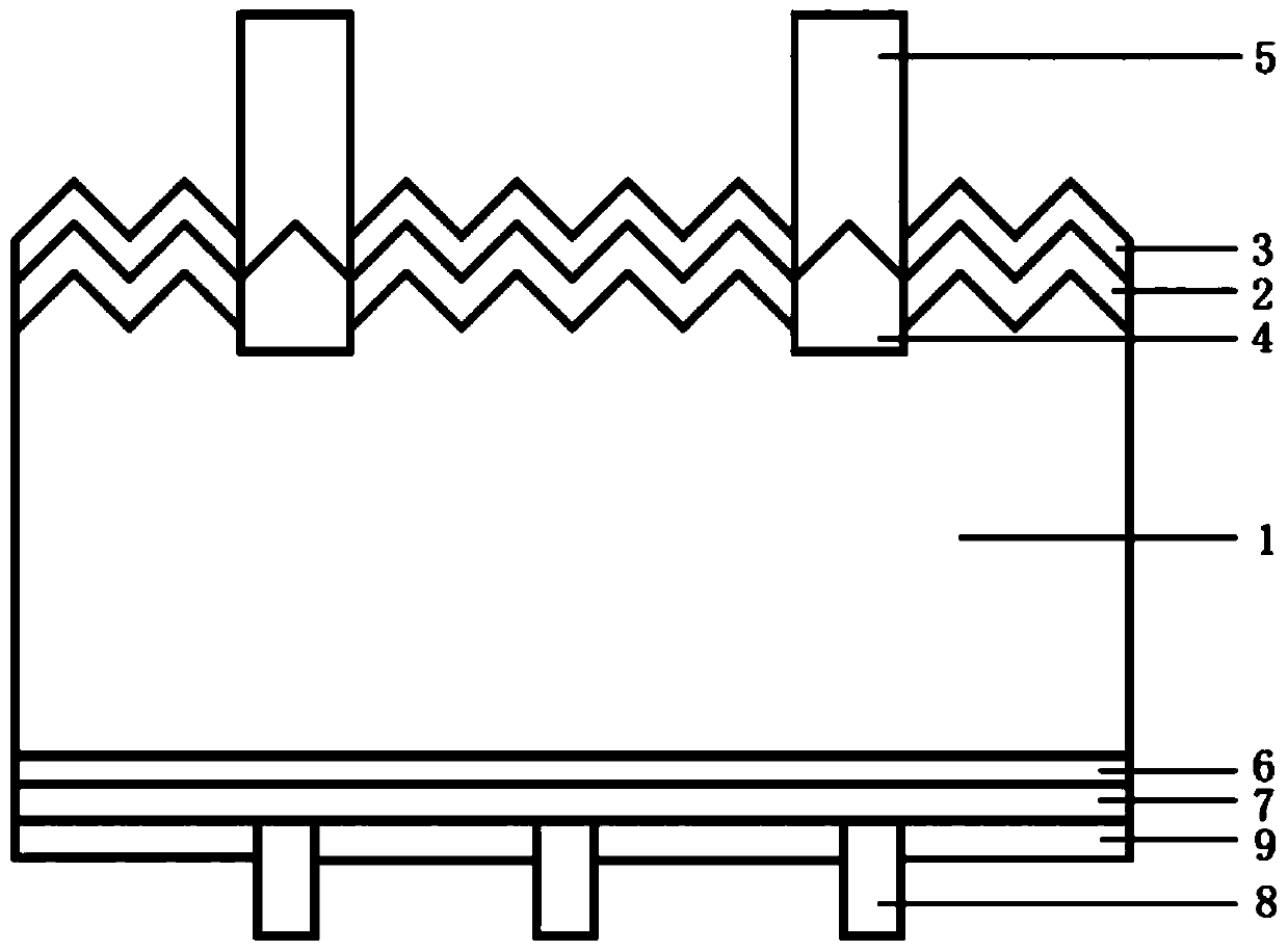
The invention discloses an n-type crystalline silicon PERT double-sided battery with a new structure and a preparation method of the n-type crystalline silicon PERT double-sided battery, and relates to the silicon solar cell field. A p + emitter layer, a hydrogenated silicon nitride antireflection layer and an Ag / Al electrode are sequentially formed on the front surface of a n-type crystalline silicon substrate, a p + + selective emitter region is locally formed on the p + emitter layer, and a silicon oxide layer, a p-doped polycrystalline silicon layer, a hydrogenated silicon nitride passivation layer and an Ag electrode are sequentially formed on the rear surface of the n-type crystalline silicon substrate. According to the present invention, the laser doping is carried out on the surface of the borosilicate glass subjected to conventional diffusion to reduce the carrier recombination of a metal contact area, and the devices, such as the low-pressure diffusion devices, etc., are notneeded for making high sheet resistance; an ultrathin silicon oxide layer with good performance is prepared in a simple, easy-to-control and extremely-low-cost nitric acid chemical oxidation mode; after the proper side insulation and high-temperature annealing processing, the characteristics of the front side structure and the rear side structure of the battery can be improved at the same time, the mutual interference is avoided, the follow-up lifting space is large, and the important significance is achieved.

Description

technical field [0001] The invention relates to the technical field of crystalline silicon solar cells, in particular to a new-structure N-type crystalline silicon PERT double-sided cell and a preparation method thereof. Background technique [0002] In recent years, the industry has paid more and more attention to n-type crystalline silicon PERT double-sided solar cells. It is a passivated emitter back surface fully diffused cell with high bulk life, high tolerance to metal impurities, and no P-type solar cells. Due to the light-induced attenuation effect caused by the boron-oxygen complex in the material, it has the advantages of 10-30% power generation gain compared with traditional single-sided solar cells. The n-PERT solar cell was first proposed by Dr. Zhao Jianhua of the University of New South Wales in Australia. IMEC in Belgium has recently optimized its laboratory technology to achieve a maximum conversion efficiency of more than 22%. Yingli, Jolywood, HT-SAAE and ...

Claims


Application Information

Patent Timeline
IPC IPC(8): H01L31/068H01L31/0368H01L31/18
CPCH01L31/03682H01L31/068H01L31/182Y02E10/546Y02P70/50
Inventor 沈文忠丁东李正平鲁贵林王暾程振东
Owner SHANGHAI JIAO TONG UNIV
Learn More