Superconducting tape suitable for non-insulated coils, non-insulated coils and preparation method thereof
A technology of superconducting tape without insulation, which is applied in the usage of superconducting elements, superconducting devices, superconducting/high-conducting conductors, etc., and can solve the problems of tape length fluctuation, batch product quality unevenness, and tape damage and other problems to achieve the effect of preventing axial sliding offset
- Summary
- Abstract
- Description
- Claims
- Application Information
AI Technical Summary
Problems solved by technology
Method used
Image
Examples
Embodiment 1
[0035] Embodiment one, metal coating:
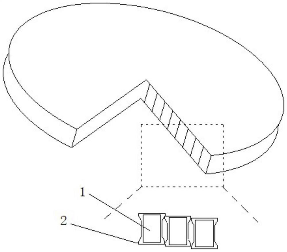
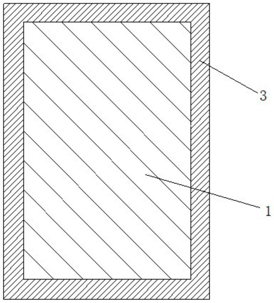
[0036] The protective layer 3 is a metal coating on the outside of the superconducting strip 1 by means of physical vapor deposition, and the metal coating may be a copper layer.
[0037] The Cu layer was prepared under the conditions of intermediate frequency magnetron sputtering, power=2.5KW, argon gas=40sccm, pressure=5mTorr, and target-base distance=7cm.
[0038] The obtained strip surface Pa is approximately equal to 200nm.
Embodiment 2
[0039] Embodiment two, metal coating:
[0040] The protective layer 3 is a metal coating on the outside of the superconducting strip 1 by electrochemical means, and the metal coating can be a copper layer.
[0041] Add a surface roughening agent into the original electroless copper plating tank for copper plating.
[0042] The obtained strip surface Pa is approximately equal to 200nm.
Embodiment 3
[0043] Embodiment three, encapsulation layer:
[0044] The protective layer 3 forms an encapsulation layer for encapsulation on the outside of the superconducting tape, and the equipment used for encapsulation can refer to the patent document CN 201710416026.8 "A Superconducting Tape Encapsulation Device".
[0045] Using 6337 solder, at a temperature of 220°C, the upper cladding strip, the superconducting strip and the lower cladding strip are simultaneously pulled into a tin furnace for extrusion molding and then pulled out.
[0046] The obtained strip surface Pa is approximately equal to 150nm.
[0047] The invention also provides a non-insulated coil, which includes a superconducting strip wound into a non-insulated coil, and a protective layer is arranged on the outer side of the superconducting strip, and the surface roughness of the protective layer is greater than Pa.
[0048] The protective layer includes: a metal plating layer or an encapsulation layer, and the metal...
PUM
 Abstract
Description
Claims
Application Information
 - R&D Engineer
- R&D Manager
- IP Professional
- Industry Leading Data Capabilities
- Powerful AI technology
- Patent DNA Extraction
Browse by: Latest US Patents, China's latest patents, Technical Efficacy Thesaurus, Application Domain, Technology Topic, Popular Technical Reports.
© 2024 PatSnap. All rights reserved.Legal|Privacy policy|Modern Slavery Act Transparency Statement|Sitemap|About US| Contact US: help@patsnap.com


