
Cleaning method for effectively removing particle agglomeration on front and back sides of wafer

A kind of particle agglomeration, front and back technology, applied in the direction of cleaning method using tools, cleaning method using liquid, cleaning method and utensils, etc., can solve the problem that the agglomerated particles are difficult to be effectively removed, reduce the output benefit of epitaxial wafers, and the cleaning process Complicated and cumbersome problems, to achieve the effect of improving the efficiency of epitaxy, improving cleaning efficiency and cleaning quality, and improving cleaning quality

Active Publication Date: 2020-01-24
SHENZHEN INST OF WIDE BANDGAP SEMICON
View PDF6 Cites 0 Cited by
  • Summary
  • Abstract
  • Description
  • Claims
  • Application Information

AI Technical Summary

Problems solved by technology

Most of the agglomerated particles are due to the van der Waals force, which has a strong force. The traditional RCA cleaning method and the dilution chemical method need to use a large amount of chemical agents for long-term soaking. , and the agglomerated particles on the front and back of the wafer after cleaning are usually difficult to be effectively removed

Method used


Image

  • Cleaning method for effectively removing particle agglomeration on front and back sides of wafer
  • Cleaning method for effectively removing particle agglomeration on front and back sides of wafer
  • Cleaning method for effectively removing particle agglomeration on front and back sides of wafer

Examples


Embodiment Construction

[0032] The implementation of the present invention will be described in detail below in conjunction with the accompanying drawings. The accompanying drawings are only for reference and description, and do not constitute a limitation to the protection scope of the present invention.

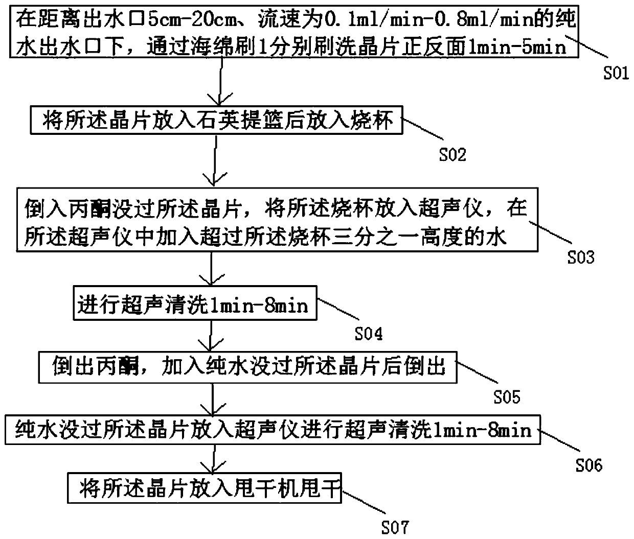
[0033] Please refer to Figure 1 to Figure 3 , a cleaning method for effectively removing particle agglomeration on the front and back sides of the wafer of the present invention, comprising the following steps:

[0034] S01, under the pure water outlet with a distance of 5cm-20cm from the water outlet and a flow rate of 0.1ml / min-0.8ml / min, use the sponge brush 1 to scrub the front and back of the wafer for 1min-5min respectively. Specifically, brush the front and back sides of the wafer with a sponge brush 1 for 1 min- It should be noted that the flow rate is controlled by a valve. Further, the sponge brush 1 includes: a long handle 11, a sponge head 12 detachably arranged at one end of the lo...


PUM

PropertyMeasurementUnit
Diameteraaaaaaaaaa
Thicknessaaaaaaaaaa
Lengthaaaaaaaaaa

Abstract

The invention relates to a semiconductor cleaning technology, in particular to a cleaning method for effectively removing particle agglomeration on the front and back sides of a wafer. The cleaning method comprises the following steps: brushing the front and back sides of the wafer with a sponge brush respectively for 1min-5min at a distance of 5cm-20cm from a pure water outlet at the flow rate of0.1 ml / min-0.8 ml / min; acetone exceeds the wafer and is put into the ultrasonic instrument for ultrasonic cleaning for 1min-8min; pouring out acetone, adding pure water and pouring it out after exceeding the wafer; repeating the step of "adding pure water and pouring it out after exceeding the wafer" for 3 times; pure water exceeds the wafer and the wafer to be put into an ultrasonic instrument for ultrasonic cleaning for 1min-8min; and the wafer is put into a spin dryer for spin drying. A single-chip fluid scouring cleaning method is adopted to quickly and effectively remove particle agglomeration on the front and back sides of the SiC wafer so as to improve the cleaning efficiency and the cleaning quality of the SiC wafer.

Description

technical field [0001] The invention relates to semiconductor cleaning technology, in particular to a cleaning method for effectively removing particle agglomeration on the front and back surfaces of a wafer. Background technique [0002] With the continuous development of the third-generation semiconductor manufacturing process, SiC wafer cleaning technology is gradually improving. During the process of grinding, polishing, epitaxy, etc., wafers are inevitably affected by the environment, personnel, equipment, tools, etc. to introduce pollutants. Among them, pollutants can be roughly classified into particles, organic matter, metal pollutants, and oxide layers. [0003] In the manufacturing process of semiconductor wafers, especially before and after the epitaxial growth process, if there are pollutants remaining on the wafer surface, it will directly cause the failure of the epitaxial wafer or the failure of the device processing. Therefore, before the wafer is epitaxy, i...

Claims


Application Information

Patent Timeline
IPC IPC(8): H01L21/02B08B1/00B08B3/08B08B3/12
CPCH01L21/02057B08B3/12B08B3/08B08B1/12
Inventor 刘福成徐悅璐孔令沂邓菁孙国胜张新河李锡光
Owner SHENZHEN INST OF WIDE BANDGAP SEMICON
Learn More