Large-gap uniform dielectric barrier discharge plasma surface treatment device under atmospheric pressure
A technology of surface treatment device and homogeneous medium, applied in the direction of plasma, electrical components, etc., can solve the problems of unfavorable electrode structure for large-area plate processing, processing material shape, thickness limitation, inability to meet special requirements, etc., to improve the processing effect, The effect of reducing breakdown field strength and high discharge power
- Summary
- Abstract
- Description
- Claims
- Application Information
AI Technical Summary
Problems solved by technology
Method used
Image
Examples
Embodiment 1
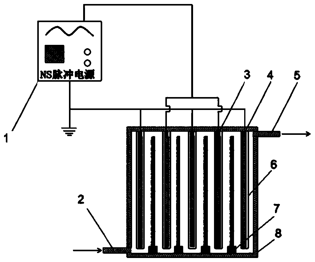
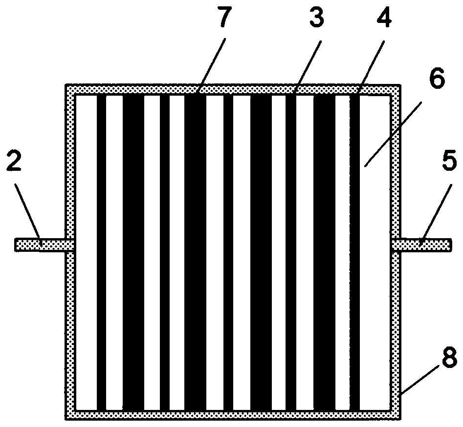
[0044] refer to figure 1 and 2 , a large-gap uniform dielectric barrier discharge plasma surface treatment device under atmospheric pressure, in a tempered glass reaction vessel with a wall thickness of 3cm, low-voltage electrodes and high-voltage electrodes covered with a 2mm quartz medium are alternately distributed, and the electrode spacing is 1cm. First, clean the PTFE surface of the material to be treated with ethanol, then place it in the air to dry naturally, then put it into the fixed slot by the airtight door, and then let the air flow in. Finally, turn on the nanosecond pulse power supply, the output voltage is 10kV, the output frequency is 2kHz, and the processing time is 5min.
Embodiment 2
[0046] refer to figure 1 and 2 , a large-gap uniform dielectric barrier discharge plasma surface treatment device under atmospheric pressure, in a tempered glass reaction vessel with a wall thickness of 3cm, low-voltage electrodes and high-voltage electrodes covered with a 2mm quartz medium are alternately distributed, and the electrode spacing is 1cm. First, use ethanol to clean the surface of the polytetrafluoroethylene of the material to be treated, then place it in the air to dry naturally, then put it into the fixed slot by the airtight door, and then pass it into argon (the argon needs to be pre-ventilated for 30 minutes) exclude air). Finally, turn on the nanosecond pulse power supply, the output voltage is 10kV, the output frequency is 2kHz, and the processing time is 5min.
Embodiment 3
[0048] refer to figure 1 and 2 , a large-gap uniform dielectric barrier discharge plasma surface treatment device under atmospheric pressure, in a tempered glass reaction vessel with a wall thickness of 3cm, low-voltage electrodes and high-voltage electrodes covered with a 2mm quartz medium are alternately distributed, and the electrode spacing is 1cm. First, use ethanol to clean the PTFE surface of the material to be treated, then place it in the air to dry naturally, then put it into the fixed slot by the airtight door, and then pass it into carbon dioxide (the carbon dioxide gas needs to be pre-ventilated for 30 minutes to get rid of it. Air). Finally, turn on the nanosecond pulse power supply, the output voltage is 10kV, the output frequency is 2kHz, and the processing time is 5min.
[0049] refer to Figure 4 , The atmospheric pressure uniform dielectric barrier discharge of different gases is introduced, which effectively improves the hydrophilicity of the surface of ...
PUM
| Property | Measurement | Unit |
|---|---|---|
| thickness | aaaaa | aaaaa |
| thickness | aaaaa | aaaaa |
Abstract
Description
Claims
Application Information
 - R&D
- Intellectual Property
- Life Sciences
- Materials
- Tech Scout
- Unparalleled Data Quality
- Higher Quality Content
- 60% Fewer Hallucinations
Browse by: Latest US Patents, China's latest patents, Technical Efficacy Thesaurus, Application Domain, Technology Topic, Popular Technical Reports.
© 2025 PatSnap. All rights reserved.Legal|Privacy policy|Modern Slavery Act Transparency Statement|Sitemap|About US| Contact US: help@patsnap.com


