A pixel structure organic light emitting diode and its preparation method
A technology of light-emitting diode and pixel structure, applied in semiconductor/solid-state device manufacturing, semiconductor devices, electrical components, etc., can solve the photon loss, can not solve the problems of OLED device efficiency roll-off, and device external quantum efficiency reduction, etc., to achieve repeated High performance, improving optical light extraction efficiency, and suppressing efficiency roll-off
- Summary
- Abstract
- Description
- Claims
- Application Information
AI Technical Summary
Problems solved by technology
Method used
Image
Examples
preparation example Construction
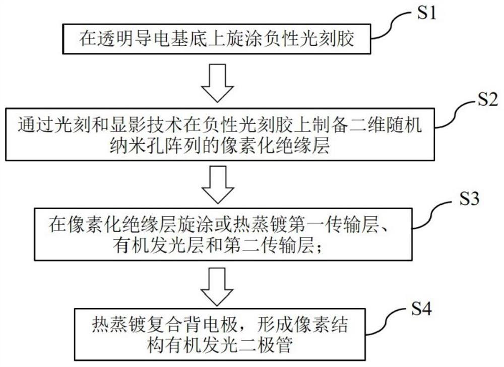
[0031] A method for preparing an organic light-emitting diode with a pixel structure, comprising the following steps:
[0032] S1. Spin-coat negative photoresist on the transparent conductive substrate 1 at 2000-3000 rpm;
[0033] S2. Prepare a pixelated insulating layer 2 of a two-dimensional random nanohole array on a negative photoresist by photolithography and development techniques;
[0034] S3, sequentially spin coating or thermally evaporating the first transport layer 3, the organic light-emitting layer 4 and the second transport layer 5 on the pixelated insulating layer 2;
[0035] S4, on the second transport layer 5 at the evaporation rate The composite back electrode 6 is thermally evaporated to form a pixel structure organic light emitting diode.
Embodiment 1
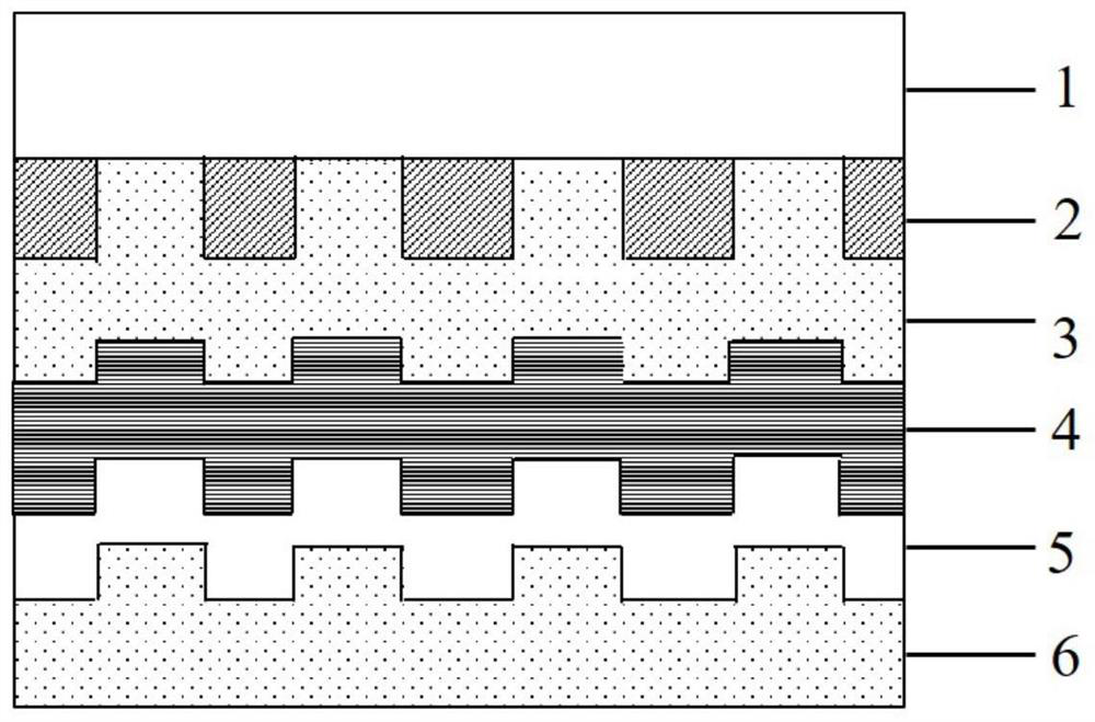
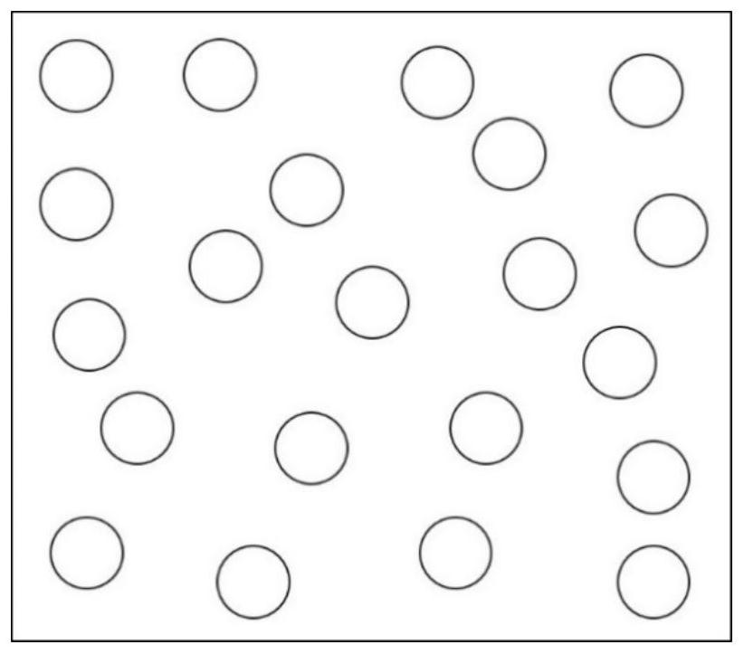
[0037] like Figure 1-4 as shown, figure 1 and figure 2 They are a structural schematic diagram of a pixel-structured organic light-emitting diode and an explanatory diagram of a manufacturing process flow, respectively, according to the present invention. Combine below Figure 1-4 , describe this embodiment in detail.
[0038] In this embodiment, a green OLED device whose luminescent material is phosphorescence is taken as an example for detailed description. like figure 1 As shown, in this structure, the transparent conductive substrate 1 is glass / ITO, the pixelated insulating layer 2 is negative photoresist (RFJ-210), and the first transmission layer 3 is N,N'-diphenyl-N , N'-(1-naphthyl)-1,1'-biphenyl-4,4'-diamine (NPB) and 4,4',4"-Tri(9-carbazoyl)triphenylamine (TCTA) A laminated structure composed of materials, the organic light-emitting layer 4 is bis(2-phenylpyridine) iridium acetylacetonate (Ir(ppy)2(acac)), and the second transport layer 5 is 1,3,5-tri[( 3-py...
Embodiment 2
[0045] Combine below Figure 1-3 and Figure 5 This embodiment will be described in detail.
[0046] In this embodiment, a green OLED device in which the luminescent material is fluorescent is taken as an example for detailed description. like figure 1 As shown, in this structure, the transparent conductive substrate 1 is glass / ITO, the pixelated insulating layer material is negative photoresist (RFJ-220), the first transmission layer 3 is an organic material NPB, the organic light-emitting layer 4 and the second Both transport layers 5 are tris (8-hydroxyquinoline) aluminum (Alq3) composite back electrode 6 is lithium fluoride (LiF) and metal aluminum (Al).
[0047] According to step S1, spin-coat negative photoresist (RFJ-220) on the transparent conductive substrate glass / ITO at 2000 rpm, and then dry it at 120 degrees Celsius.
[0048] According to step S2, after exposing the mask with an argon ion laser, develop in a sodium hydroxide (NaOH) solution with a volume fract...
PUM
| Property | Measurement | Unit |
|---|---|---|
| thickness | aaaaa | aaaaa |
Abstract
Description
Claims
Application Information
 - R&D Engineer
- R&D Manager
- IP Professional
- Industry Leading Data Capabilities
- Powerful AI technology
- Patent DNA Extraction
Browse by: Latest US Patents, China's latest patents, Technical Efficacy Thesaurus, Application Domain, Technology Topic, Popular Technical Reports.
© 2024 PatSnap. All rights reserved.Legal|Privacy policy|Modern Slavery Act Transparency Statement|Sitemap|About US| Contact US: help@patsnap.com


