
Phosphorescent OLED device and manufacturing method thereof

A manufacturing method, phosphorescence technology, applied in semiconductor/solid-state device manufacturing, electrical solid-state devices, semiconductor devices, etc., can solve the problems of complex doping process, efficiency roll-off, difficult precise control, etc., and achieve simple manufacturing process and suppression efficiency roll-off effect

Inactive Publication Date: 2019-05-21
AAC TECH NANJING
View PDF5 Cites 0 Cited by
  • Summary
  • Abstract
  • Description
  • Claims
  • Application Information

AI Technical Summary

Problems solved by technology

[0005] However, the inventors of the present invention have found that: in order to realize triplet phosphorescence when making phosphorescent OLED devices, it is usually necessary to dope heavy metal atoms and host materials. Phosphorescence lifetime is relatively long, which is prone to concentration quenching and triplet-triplet annihilation (TTA), resulting in severe efficiency roll-off

Method used


Image

  • Phosphorescent OLED device and manufacturing method thereof
  • Phosphorescent OLED device and manufacturing method thereof
  • Phosphorescent OLED device and manufacturing method thereof

Examples


Embodiment Construction

[0023] In order to make the objectives, technical solutions, and advantages of the embodiments of the present invention clearer, the embodiments of the present invention will be described in detail below with reference to the accompanying drawings. However, a person of ordinary skill in the art can understand that, in each embodiment of the present invention, many technical details are proposed for the reader to better understand the present invention. However, even without these technical details and various changes and modifications based on the following embodiments, the technical solution claimed by the present invention can be realized.

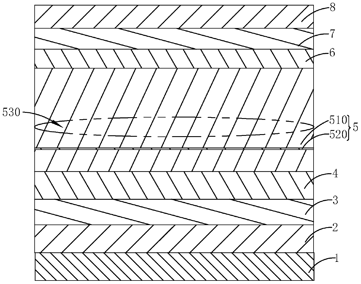
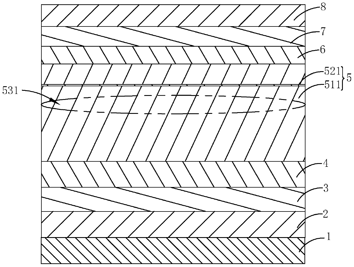
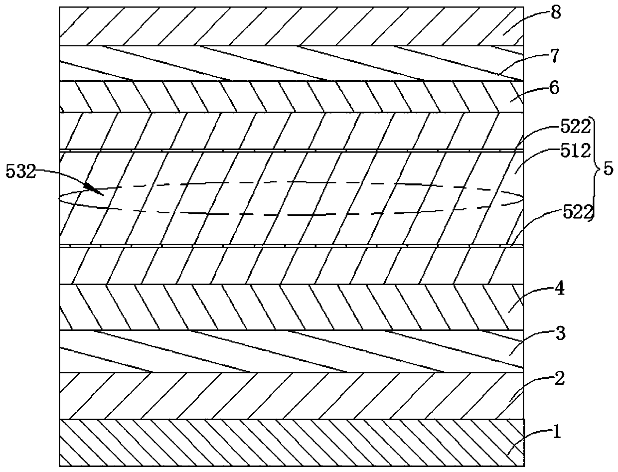
[0024] The first embodiment of the present invention relates to a phosphorescent OLED device, such as figure 1 As shown, the core of this embodiment is to include: a substrate 1, and an anode layer 2, a hole injection layer 3, a hole transport layer 4, an organic light-emitting layer 5, an electron transport layer 6, and an electron injectio...


PUM


Abstract

The embodiment of the invention relates to the technical field of display, and discloses a phosphorescent OLED device. The phosphorescent device comprises a substrate and a positive electrode layer, ahole injection layer, a hole transmission layer, an organic light-emitting layer, an electron transmission layer, an electron injection layer and a negative electrode layer which sequentially arranged on the substrate, the organic light-emitting layer is a non-doing type and comprises a non-doping main body layer and a non-doping phosphorescent light-emitting layer, and the non-doping phosphorescent light-emitting layer is embedded into the non-doping main body layer. The phosphorescent OLED device and the manufacturing method, provided by the embodiment of the invention are simple in processand high in practicability, and the efficiency roll-off can be effectively prevented.

Description

Technical field [0001] The embodiments of the present invention relate to the field of display technology, in particular to a phosphorescent OLED device and a manufacturing method thereof. Background technique [0002] At present, OLED display technology is becoming more and more mature, and commercial products have entered people's field of vision. The OLED display technology is composed of very thin organic material film layers and substrates. These organic materials will emit light when a charge passes through the organic material film layer. The color of the OLED device's light emission depends on the material of the organic light-emitting layer, which can be changed by changing the light-emitting layer. Dye materials to get the desired color. [0003] OLED device displays have the advantages of self-luminescence, simple structure, high contrast, thin thickness, wide viewing angle, fast response speed, low power consumption, and wide operating temperature range. If a flexible ...

Claims


Application Information

Patent Timeline
Patent Type & Authority Applications(China)
IPC IPC(8): H01L51/50H01L51/56
Inventor 孙霞
Owner AAC TECH NANJING
Learn More