
Thermally-induced delayed fluorescence semiconductor, and preparation method and application thereof

A thermally-induced delayed fluorescence, semiconductor technology, applied in semiconductor/solid-state device manufacturing, semiconductor devices, chemical instruments and methods, etc., can solve the problems of poor color purity, wide EL spectrum, missing spectral fine structure, etc.

Pending Publication Date: 2021-09-03
NANJING UNIV OF POSTS & TELECOMM
View PDF3 Cites 0 Cited by
  • Summary
  • Abstract
  • Description
  • Claims
  • Application Information

AI Technical Summary

Problems solved by technology

Usually, the existence of ICT causes the spectrum of molecular excited state to radiate to the ground state to broaden, and the spectral fine structure is missing. Therefore, the PLQY of TADF materials (regardless of blue light, green light or red light) can be very high, even close to 100 %, the color purity is often poor, and the effective use of TADF can overcome the forbidden selection law, capture excitons to achieve high luminous efficiency, and overcome the problem of wide EL spectrum of TADFOLED devices

Method used

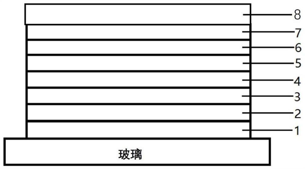
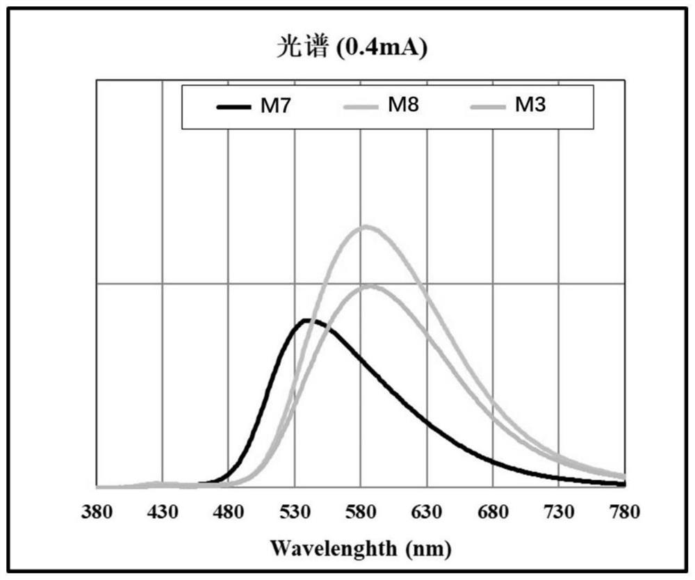

Image

  • Thermally-induced delayed fluorescence semiconductor, and preparation method and application thereof
  • Thermally-induced delayed fluorescence semiconductor, and preparation method and application thereof
  • Thermally-induced delayed fluorescence semiconductor, and preparation method and application thereof

Examples


preparation example Construction

[0065] The present invention also discloses a method for preparing thermally induced delayed fluorescent semiconductors. The preparation method includes the following steps: the intermediate raw material F1-1 undergoes boronate or borate reaction to obtain intermediate raw materials F1-3, F1-2 and F1 -3 is coupled under catalytic conditions to obtain F1-4, and then undergoes ester hydrolysis to obtain F1-5, and F1-5 undergoes ring-closing reaction to obtain F1-6.

[0066]

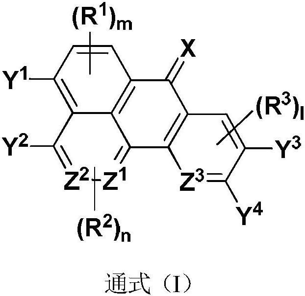
[0067] A of each intermediate diagram in the above steps 1 、A 2 , B 1 , B 2 ,Z 1 ~ Z 3 , R 1 ~R 3 , 1, m, n and Y in the general formula (I) 1 ~Y 4 ,Z 1 ~ Z 3 , R 1 ~R 3 , l, m, n each independently have the same limited range, A 3 and B 3 Each independently represents one of chlorine, bromine or iodine, and Ra represents one of methyl, ethyl or tert-butyl.

[0068] When necessary, the A in F1-6 1 、A 2 , B 1 , B 2 F1-7 can be obtained through C-C coupling reaction or C-N coupling react...

Embodiment 1

[0074] The present embodiment provides species having the structure shown in the following formula M1:

[0075]

[0076] The synthetic route of M1:

[0077]

[0078] Synthesis of compound 1: 1,5-dibromo-2,6-dimethylnaphthalene (5g, 15.9mmol), biboronic acid pinacol ester (4.8g, 19mmol), potassium acetate (4.7g, 48mmol) 1 , 1'-bisdiphenylphosphinoferrocenepalladium dichloride (20mg) was placed in a two-necked flask, after flushing nitrogen for three times, 25mL of anhydrous dimethyl sulfoxide was added; the reaction was carried out under nitrogen protection, 80 After reacting at ℃ for 8 hours, after the completion of the reaction, the reaction was cooled to room temperature, poured into water, and suction filtered to obtain a filter cake as a crude product. The crude product was obtained by column chromatography to obtain compound 1 with a mass of 4.31 g. The yield was 75%.

[0079] Synthesis of Compound 2: Put Compound 1 (4g, 11mmol), methyl 2,5-dibromobenzoate (3.55g,...

Embodiment 2

[0084] The present embodiment provides the species with the structure shown in the following formula M2:

[0085]

[0086] The synthetic route of M2:

[0087]

[0088] Synthesis of compound 1: 1,5-dibromo-2,6-dimethylnaphthalene (5g, 15.9mmol), biboronic acid pinacol ester (4.8g, 19mmol), potassium acetate (4.7g, 48mmol) 1 , 1'-bisdiphenylphosphinoferrocenepalladium dichloride (20mg) was placed in a two-necked flask, after flushing nitrogen for three times, 25mL of anhydrous dimethyl sulfoxide was added; the reaction was carried out under nitrogen protection, 80 After reacting at ℃ for 8 hours, after the completion of the reaction, the reaction was cooled to room temperature, poured into water, and suction filtered to obtain a filter cake as a crude product. The crude product was obtained by column chromatography to obtain compound 1 with a mass of 4.31 g. The yield was 75%.

[0089] Synthesis of Compound 2: Put Compound 1 (4g, 11mmol), methyl 2,5-dibromobenzoate (3.55...


PUM


Abstract

The invention discloses a thermally-induced delayed fluorescence semiconductor, and a preparation method and application thereof. The thermally-induced delayed fluorescence semiconductor uses polycyclic aromatic hydrocarbon containing electron withdrawing groups as a molecular mother nucleus to construct a novel organic electroluminescent material, and material molecules have high triplet state energy level, high PLQY and high glass transition temperature. When the thermally-induced delayed fluorescence material is used as a light-emitting material of a light-emitting layer, due to the high triplet state energy level, effective energy transfer from a host material to a guest material can be promoted, energy return is reduced, and the light-emitting efficiency of an OLED device is improved. The HOMO energy level of the thermally-induced delayed fluorescent material is high, the Fermi energy level matching performance of the thermally-induced delayed fluorescent material with a hole injection layer and a hole transport layer is improved, the hole injection performance of material molecules is further improved, meanwhile, a planar rigid framework of the molecules is beneficial to charge transport, the turn-on voltage of a related electroluminescent device can be very efficiently reduced, and the current efficiency under high current density is maintained.

Description

technical field [0001] The invention relates to a heat-induced delayed fluorescent semiconductor and its preparation method and application, which can be used in the technical field of organic electroluminescent materials. Background technique [0002] After nearly 20 years of development, organic light-emitting diodes have successfully entered the commercialization stage, and have been chased by global industrial capital in lighting, display and other fields. The core parameters of color organic light-emitting diode devices mainly include high color purity, high brightness, long life, low turn-on voltage, and wide color gamut. The multi-layer structure of light-emitting diode devices makes it necessary to meet these device indicators, and it is necessary to simultaneously obtain the best performance in multiple research fields such as luminescent materials, transport layer materials, electrode materials, device structures, and device processing techniques. The key steps of...

Claims


Application Information

Patent Timeline
Patent Type & Authority Applications(China)
IPC IPC(8): C07C225/22C07C255/42C07C255/58C07D221/18C07D307/91C09K11/06H01L51/54H01L51/50
CPCC07C225/22C07C255/42C07C255/58C07D307/91C07D221/18C09K11/06C09K2211/1007C09K2211/1014C09K2211/1011C09K2211/1029C09K2211/1088H10K85/622H10K85/631H10K85/636H10K85/626H10K85/633H10K85/654H10K85/6572H10K85/6574H10K50/11
Inventor 傅妮娜李学伟汪联辉田梦李海洋
Owner NANJING UNIV OF POSTS & TELECOMM
Learn More